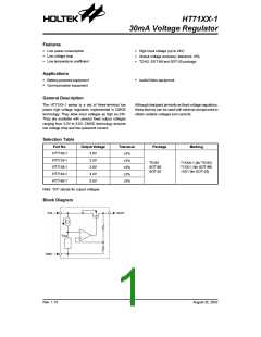
HT71XX-1
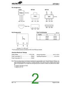
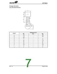
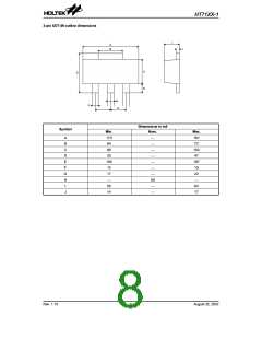
Pin Assignment
T
O
-
9
2
S
O
T
-
8
9
S
O
T
-
2
5
N
C
N
C
ꢀ
r
o
n
t
V
i
e
w
7
1
X
X
A
-
1
7
1
X
X
-
1
T
o
p
V
i
e
w
1
X
X
1
G
N
D
V
I
N
V
O
U
T
G
N
D
V
I
N
V
O
U
T
G
N
D
V
I
N
V
O
U
T
B
o
t
t
o
m
V
i
e
w
G
N
D
V
I
N
V
O
U
T
G
N
D
V
I
N
V
O
U
T
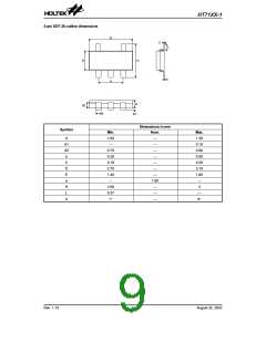
Pad Assignment
Pad Coordinates
Unit: mm
Pad No.
X
Y
1
2
3
-429.00
123.50
416.00
-401.00
-401.00
-401.00
(
0
,
0
)
2
3
1
Chip size: 1111´1051 (mm)2
* The IC substrate should be connected to VDD in the PCB layout artwork.
Absolute Maximum Ratings
Supply Voltage .........................................-0.3V to 26V
Power Consumption (*1) .................................. 200mW
Power Consumption (*2) ...................................150mW
Storage Temperature ...........................-50°C to 125°C
Operating Temperature ..............................0°C to 70°C
Note: These are stress ratings only. Stresses exceeding the range specified under ²Absolute Maximum Ratings² may
cause substantial damage to the device. Functional operation of this device at other conditions beyond those
listed in the specification is not implied and prolonged exposure to extreme conditions may affect device reliabil-
ity.
*1: applied to SOT-89 and TO-92
*2: applied to SOT-25
Rev. 1.10
2
August 22, 2002

 HOLTEK [ HOLTEK SEMICONDUCTOR INC ]