HT46RU66/HT46CU66
Configuration
Option
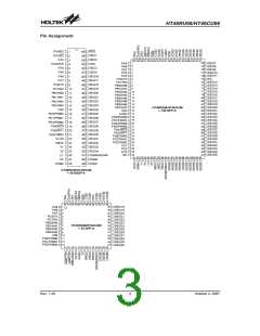
Pin Name
VREF
I/O
Description
I
I
Reference voltage input pin.
¾
¾
¾
¾
¾
¾
RES
Schmitt Trigger reset input. Active low.
Positive power supply
VDD
¾
¾
I
VSS
Negative power supply, ground
Positive analog power supply
Negative analog power supply, ground
AVDD
AVSS
I
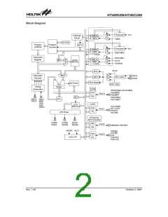
Note: Each pin on Port A can be programmed through a configuration option to have a wake-up function.
Individual pins can be selected to have a pull-high resistor.
Pins V2, C1, C2 and segment pin SEG34 are not available on the 52-pin QFP package.
Pins PB4/AN4~PB7/AN7 only exist on the 100-pin QFP package.
Pins PC0~PC5 only exist on the 100-pin QFP package.
Pin PD3/PWM3 only exists on the 100-pin QFP package.
Pins PD7/TMR1 and PC0/TMR2 only exist on the 100-pin QFP package. The 56-pin SSOP and 52-pin QFP
packages have only one external timer input TMR0.
Segment pins SEG0~SEG15 and SEG35~SEG45 only exist on the 100-pin QFP package.
For the 52-pin QFP and 56-pin SSOP, the VREF, AVDD are bonded together with VDD pin.
For the 52-pin QFP and 56-pin SSOP, the AVSS is bonded together with VSS pin.
Absolute Maximum Ratings
Supply Voltage...........................VSS-0.3V to VSS+6.0V
Input Voltage..............................VSS-0.3V to VDD+0.3V
Storage Temperature............................-50°C to 125°C
Operating Temperature...........................-40°C to 85°C
IOH Total............................................................-100mA
I
OL Total ..............................................................150mA
Total Power Dissipation .....................................500mW
Note: These are stress ratings only. Stresses exceeding the range specified under ²Absolute Maximum Ratings² may
cause substantial damage to the device. Functional operation of this device at other conditions beyond those listed
in the specification is not implied and prolonged exposure to extreme conditions may affect device reliability.
D.C. Characteristics
Ta=25°C
Test Conditions
Conditions
Symbol
Parameter
Min.
Typ.
Max.
Unit
VDD
¾
fSYS=4MHz
SYS=8MHz
2.2
3.3
5.5
5.5
V
V
¾
¾
VDD
Operating Voltage
f
¾
Analog Operating Voltage
(see Note 5)
AVDD
VREF=AVDD
3.0
5.5
V
¾
¾
3V
5V
3V
5V
1
3
2
5
3
6
mA
mA
mA
mA
¾
¾
¾
¾
Operating Current
No load, fSYS=4MHz,
ADC Off, UART Off
IDD1
(Crystal OSC, RC OSC)
1.5
3
Operating Current
No load, fSYS=4MHz,
ADC Off, UART On
IDD2
(Crystal OSC, RC OSC)
Operating Current
No load, fSYS=8MHz,
ADC Off, UART Off
IDD3
5V
5V
4
5
8
mA
mA
¾
¾
(Crystal OSC, RC OSC)
Operating Current
No load, fSYS=8MHz,
ADC Off, UART On
IDD4
10
(Crystal OSC, RC OSC)
3V
5V
0.3
0.6
0.6
1
mA
mA
¾
¾
Operating Current
(fSYS=32768Hz)
No load, ADC Off,
UART Off
IDD5
Rev. 1.20
5
October 2, 2007

 HOLTEK [ HOLTEK SEMICONDUCTOR INC ]