HT46R23/HT46C23
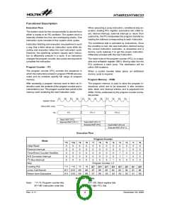
If the stack is full and a non-masked interrupt takes
place, the interrupt request flag will be recorded but the
acknowledgment will be inhibited. When the stack
pointer is decremented (by RET or RETI), the interrupt
will be serviced. This feature prevents stack overflow al-
lowing the programmer to use the structure more easily.
In a similar case, if the stack is full and a ²CALL² is sub-
sequently executed, stack overflow occurs and the first
entry will be lost (only the most recent 8 return ad-
dresses are stored).
The memory pointer registers (MP0 and MP1 are 8-bit
registers).
Accumulator
The accumulator is closely related to ALU operations. It
is also mapped to location 05H of the data memory and
can carry out immediate data operations. The data
movement between two data memory locations must
pass through the accumulator.
I
n
d
i
r
e
c
t
A
d
d
r
e
s
s
i
n
g
R
e
g
i
s
t
e
r
0
0
0
0
0
0
0
0
0
0
0
0
1
2
3
4
5
6
7
8
9
H
H
H
H
H
H
H
H
H
H
Data Memory - RAM
M
e
M
P
0
I
n
d
i
r
e
c
t
A
d
d
r
s
s
i
n
g
R
e
g
i
s
t
e
r
1
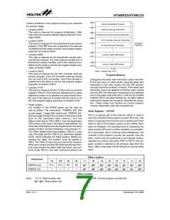
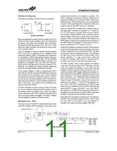
The data memory is designed with 224´8 bits. The
data memory is divided into two functional groups: spe-
cial function registers and general purpose data mem-
ory (192´8). Most are read/write, but some are read
only.
P
1
A
C
C
P
C
L
T
B
L
P
T
B
L
H
The special function registers include the indirect ad-
dressing registers (00H;02H), timer/event counter
higher-order byte register (TMRH;0CH), timer/event
counter low-order byte register (TMRL;0DH),
timer/event counter control register (TMRC;0EH), pro-
gram counter lower-order byte register (PCL;06H),
memory pointer registers (MP0;01H, MP1;03H), accu-
mulator (ACC;05H), table pointer (TBLP;07H), table
higher-order byte register (TBLH;08H), status register
(STATUS;0AH), interrupt control register 0 (INTC0;
0BH), PWM data register (PWM0;1AH, PWM1;1BH),
the I2C Bus slave address register (HADR;20H), the I2C
Bus control register (HCR;21H), the I2C Bus status reg-
ister (HSR;22H), the I2C Bus data register (HDR;23H),
the A/D result lower-order byte register (ADRL;24H), the
A/D result higher-order byte register (ADRH;25H), the
A/D control register (ADCR;26H), the A/D clock setting
register (ACSR;27H), I/O registers (PA;12H, PB;14H,
PC;16H, PD;18H) and I/O control registers (PAC;13H,
PBC;15H, PCC;17H, PDC;19H). The remaining space
before the 40H is reserved for future expanded usage
and reading these locations will get ²00H². The general
purpose data memory, addressed from 40H to FFH, is
used for data and control information under instruction
commands.
0
0
A
B
H
H
S
T
A
T
U
S
I
T
N
T
C
0
0
0
C
D
H
H
M
R
H
T
M
R
L
0
E
H
T
M
R
C
0
F
H
H
H
H
H
H
H
H
H
H
H
1
1
1
1
1
1
1
1
1
1
0
1
2
3
4
5
6
7
8
9
P
A
P
A
C
S
p
e
c
i
a
l
P
u
r
p
o
s
e
D
a
t
a
M
e
m
o
r
y
P
B
P
B
C
P
P
C
P
P
C
D
C
C
D
1
1
A
B
H
H
P
P
W
W
M
M
0
1
1
1
C
D
H
H
1
E
H
I
N
T
C
1
1
F
H
H
H
H
H
H
H
H
H
2
2
2
2
2
2
2
2
0
1
2
3
4
5
6
7
H
A
D
R
H
C
R
H
S
R
H
D
R
All of the data memory areas can handle arithmetic,
logic, increment, decrement and rotate operations di-
rectly. Except for some dedicated bits, each bit in the
data memory can be set and reset by ²SET [m].i² and
²CLR [m].i². They are also indirectly accessible through
memory pointer registers (MP0;01H/MP1;03H).
A
D
R
L
A
A
D
D
R
C
H
R
A
C
S
R
2
8
H
3
F
H
4
0
H
Indirect Addressing Register
G
e
n
e
r
a
l
P
u
r
p
o
s
e
:
U
n
u
s
e
d
D
a
t
a
M
e
m
o
r
y
Location 00H and 02H are indirect addressing registers
that are not physically implemented. Any read/write op-
eration of [00H] or [02H] will access data memory
pointed to by MP0[01H] or MP1[03H] respectively.
Reading location 00H or 02H itself indirectly will return
the result 00H. Writing indirectly result in no operation.
R
e
a
d
a
s
"
0
0
"
(
1
9
2
B
y
t
e
s
)
F
F
H
RAM Mapping
Rev. 2.11
8
December 29, 2008
图片预览")
 HOLTEK [ HOLTEK SEMICONDUCTOR INC ]