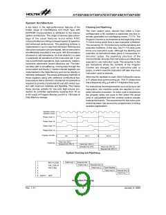
HT46F46E/HT46F47E/HT46F48E/HT46F49E
Pin Description
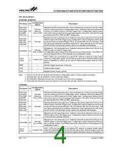
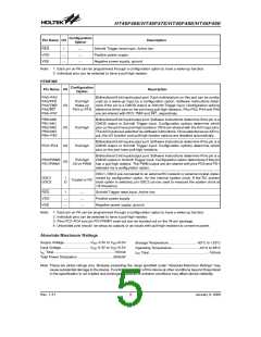
HT46F46E, HT46F47E
Configuration
Pin Name I/O
Description
Option
PA0~PA2
PA3/PFD
Bidirectional 8-bit input/output port. Each individual pin on this port can be config-
ured as a wake-up input by a configuration option. Software instructions determine
if the pin is a CMOS output or Schmitt Trigger input. Configuration options deter-
Pull-high
Wake-up
PA4/TMR I/O
PA5/INT
PA3 or PFD mine which pins on the port have pull-high resistors. Pins PA3, PA4 and PA5 are
pin-shared with PFD, TMR and INT, respectively.
PA6~PA7
Bidirectional 4-bit input/output port. Software instructions determine if the pin is a
CMOS output or Schmitt Trigger input. Configuration options determine which pins
PB0/AN0
PB1/AN1
I/O
Pull-high
on the port have pull-high resistors. PB is pin-shared with the A/D input pins. The
A/D inputs are selected via software instructions. Once selected as an A/D input,
the I/O function and pull-high resistor options are disabled automatically.
PB2/AN2
PB3/AN3
Bidirectional 1-bit input/output port. Software instructions determine if the pin is a
CMOS output or Schmitt Trigger input.
Pull-high
PD0/PWM I/O
PD0 or PWM A configuration option determines if this pin has a pull-high resistor. The PWM out-
put is pin-shared with pin PD0 selected via a configuration option.
OSC1, OSC2 are connected to an external RC network or external crystal, deter-
OSC1
OSC2
I
mined by configuration option, for the internal system clock. If the RC system clock
Crystal or RC
O
option is selected, pin OSC2 can be used to measure the system clock at 1/4 fre-
quency.
RES
VDD
VSS
I
Schmitt Trigger reset input. Active low.
Positive power supply
¾
¾
¾
¾
¾
Negative power supply, ground
Note: 1. Each pin on PA can be programmed through a configuration option to have a wake-up function.
2. Individual pins can be selected to have a pull-high resistor.
3. Pins PB2/AN2~PB3/AN3 exist but are not bonded out on the 16-pin package.
4. Unbonded pins should be setup as outputs or as inputs with pull-high resistors to conserve power.
HT46F48E
Configuration
Pin Name I/O
Description
Option
PA0~PA2
PA3/PFD
Bidirectional 8-bit input/output port. Each individual pin on this port can be config-
ured as a wake-up input by a configuration option. Software instructions determine
if the pin is a CMOS output or Schmitt Trigger input. Configuration options deter-
Pull-high
Wake-up
PA4/TMR I/O
PA5/INT
PA3 or PFD mine which pins on the port have pull-high resistors. Pins PA3, PA4 and PA5 are
pin-shared with PFD, TMR and INT, respectively.
PA6~PA7
PB0/AN0
Bidirectional 8-bit input/output port. Software instructions determine if the pin is a
CMOS output or Schmitt Trigger input. Configuration options determine which pins
PB1/AN1
PB2/AN2 I/O
PB3/AN3
Pull-high
on the port have pull-high resistors. PB is pin-shared with the A/D input pins. The
A/D inputs are selected via software instructions. Once selected as an A/D input,
the I/O function and pull-high resistor options are disabled automatically.
PB4~PB7
Bidirectional 2-bit input/output port. Software instructions determine if the pin is a
CMOS output or Schmitt Trigger input. Configuration options determine which pins
on the port have pull-high resistors.
PC0~PC1 I/O
PD0/PWM I/O
Pull-high
Pull-high
Bidirectional 1-bit input/output port. Software instructions determine if the pin is a
CMOS output or Schmitt Trigger input. Configuration option determines if this pin
I/O or PWM has a pull-high resistor. The PWM output is pin-shared with pin PD0 selected via a
configuration option.
OSC1, OSC2 are connected to an external RC network or external crystal, deter-
Crystal or RC mined by configuration option, for the internal system clock. If the RC system clock op-
tion is selected, pin OSC2 can be used to measure the system clock at 1/4 frequency.
OSC1
OSC2
I
O
Rev. 1.31
4
January 9, 2009
图片预览")
 HOLTEK [ HOLTEK SEMICONDUCTOR INC ]