HT46F46E/HT46F47E/HT46F48E/HT46F49E
READ
WRITE
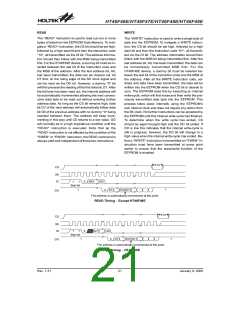
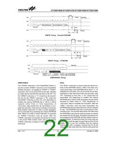
The ²READ² instruction is used to read out one or more
bytes of data from the EEPROM Data Memory. To insti-
gate a ²READ² instruction, the CS bit should be set high,
followed by a high start bit and then the instruction code
²10², all transmitted via the DI bit. The address informa-
tion should then follow with the MSB being transmitted
first. For the HT46F49E device, a dummy bit must be in-
serted between the last bit of the instruction code and
the MSB of the address. After the last address bit, A0,
has been transmitted, the data can be clocked out, bit
D7 first, on the rising edge of the SK clock signal and
can be read via the DO bit. However, a dummy ²0² bit
will first precede the reading of the first data bit, D7. After
the full byte has been read out, the internal address will
be automatically incremented allowing the next consec-
utive data byte to be read out without entering further
address data. As long as the CS bit remains high, data
bit D7 of the next address will automatically follow data
bit D0 of the previous address with no dummy ²0² being
inserted between them. The address will keep incre-
menting in this way until CS returns to a low value. DO
will normally be in a high impedance condition until the
²READ² instruction is executed. Note that as the
²READ² instruction is not affected by the condition of the
²EWEN² or ²EWDS² instruction, the READ command is
always valid and independent of these two instructions.
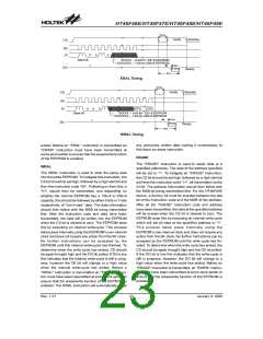
The ²WRITE² instruction is used to write a single byte of
data into the EEPROM. To instigate a WRITE instruc-
tion, the CS bit should be set high, followed by a high
start bit and then the instruction code ²01², all transmit-
ted via the DI bit. The address information should then
follow with the MSB bit being transmitted first. After the
last address bit, A0, has been transmitted, the data can
be immediately transmitted MSB first. For the
HT46F49E device, a dummy bit must be inserted be-
tween the last bit of the instruction code and the MSB of
the address. After all the WRITE instruction code, ad-
dress and data have been transmitted, the data will be
written into the EEPROM when the CS bit is cleared to
zero. The EEPROM does this by executing an internal
write-cycle, which will first erase and then write the pre-
viously transmitted data byte into the EEPROM. This
process takes place internally using the EEPROM¢s
own internal clock and does not require any action from
the SK clock. No further instructions can be accepted by
the EEPROM until this internal write-cycle has finished.
To determine when the write cycle has ended, CS
should be again brought high and the DO bit polled. If
DO is low this indicates that the internal write-cycle is
still in progress, however, the DO bit will change to a
high value when the internal write-cycle has ended. Be-
fore a ²WRITE² instruction is transmitted an ²EWEN² in-
struction must have been transmitted at some point
earlier to ensure that the erase/write function of the
EEPROM is enabled.
t
C D S
C
S
S
K
D
I
0
A
6
A
0
1
1
S
t
a
r
t
b
i
t
1
1
0
D
7
D
0
D
7
D
O
T
h
e
a
d
d
r
e
s
s
i
s
a
u
t
o
m
a
t
i
c
a
l
l
y
i
n
c
r
e
m
e
n
t
e
d
a
t
t
h
i
s
p
o
i
n
t
.
READ Timing - Except HT46F49E
t
C
D
S
C
S
S
K
D
I
1
1
0
A
7
A
0
S
t
a
r
t
b
i
t
1
0
D
7
D
0
D
7
1
D
O
T
h
e
a
d
d
r
e
s
s
i
s
a
u
t
o
m
a
t
i
c
a
l
l
y
i
n
c
r
e
m
e
n
t
e
d
a
t
t
h
i
s
p
o
i
n
t
.
READ Timing - HT46F49E
Rev. 1.31
21
January 9, 2009
图片预览")
 HOLTEK [ HOLTEK SEMICONDUCTOR INC ]