HT36F2
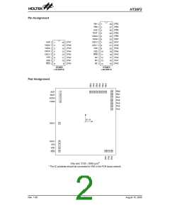
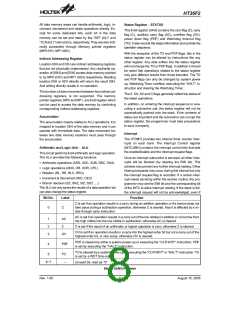
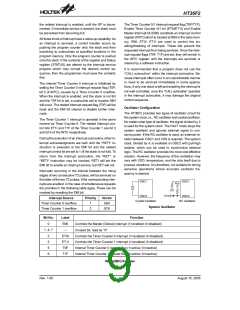
Pad Coordinates
Unit: mm
Pad No.
X
Y
Pad No.
X
Y
1
2
1043.000
931.200
817.560
715.600
14
15
16
17
18
19
20
21
22
23
24
25
916.350
916.350
916.350
916.350
916.350
916.350
704.250
593.650
493.650
383.050
283.050
172.450
514.500
625.100
725.100
835.700
935.700
1046.300
1041.550
1041.550
1041.550
1041.550
1041.550
1041.550
-876.150
-876.150
-876.150
-876.150
-916.350
-916.350
-916.350
-916.350
-916.350
710.500
3
4
5
-63.124
-740.976
-842.650
-942.650
-1044.324
-1041.350
-1041.350
-1041.350
414.500
6
7
8
9
10
11
12
13
810.500
921.100
916.350
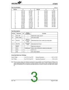
Pad Description
Internal
Connection
Pad No.
Pad Name
I/O
Function
8, 7
3,4
VDD, VSS
Digital power supply, ground
DAC power supply
¾
¾
¾
VDDA, VSSA
¾
Wake-up,
10~17
25~18
PA0~PA7
I/O
Pull-high or Bidirectional 8-bit I/O port, wake-up by mask option
None
Pull-high or
PB0~PB7
I/O
Bidirectional 8-bit I/O port
None
9
6
5
1
RESET
OSC1
OSC2
AUD
I
Reset input, active low
X¢tal/Resistor XIN for X¢tal or ROSCIN for resistor by mask option
¾
I
O
O
XOUT or T1
¾
¾
DAC output interface
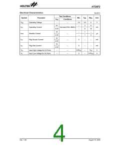
Absolute Maximum Ratings
Supply Voltage ..........................VSS-0.3V to VSS+5.5V
Input Voltage .............................VSS-0.3V to VDD+0.3V
Storage Temperature ...........................-50°C to 125°C
Operating Temperature ..........................-25°C to 70°C
Note: These are stress ratings only. Stresses exceeding the range specified under ²Absolute Maximum Ratings² may
cause substantial damage to the device. Functional operation of this device at other conditions beyond those
listed in the specification is not implied and prolonged exposure to extreme conditions may affect device reliabil-
ity.
Rev. 1.00
3
August 15, 2005

 HOLTEK [ HOLTEK SEMICONDUCTOR INC ]