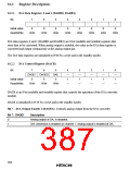
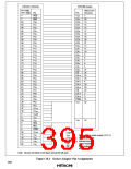
17.1.2 RAM Enable Bit (RAME) in System Control Register (SYSCR)
Bit
7
SSBY
0
6
STS2
0
5
STS1
0
4
STS0
0
3
XRST
1
2
NMIEG
0
1
HIE
0
0
RAME
1
Initial value
Read/Write
R/W
R/W
R/W
R/W
R
R/W
R/W
R/W
The on-chip RAM is enabled or disabled by the RAME bit in SYSCR. See section 3.2, System
Control Register (SYSCR), for the other SYSCR bits.
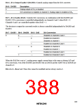
Bit 0—RAM Enable (RAME): This bit enables or disables the on-chip RAM. The RAME bit is
initialized to 1 on the rising edge of the RES signal. The RAME bit is not initialized in software
standby mode.
Bit 0: RAME
Description
0
1
On-chip RAM is disabled.
On-chip RAM is enabled.
(Initial value)
17.2
Operation
17.2.1 Expanded Modes (Modes 1 and 2)
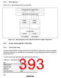
If the RAME bit is set to 1, accesses to addresses H'F780 to H'FF7F in the H8/3437 and H8/3436
and addresses H'FB80 to H'FF7F in the H8/3434 are directed to the on-chip RAM. If the RAME
bit is cleared to 0, accesses to these addresses are directed to the external data bus.
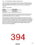
17.2.2 Single-Chip Mode (Mode 3)
If the RAME bit is set to 1, accesses to addresses H'F780 to H'FF7F in the H8/3437 and H8/3436
and addresses H'FB80 to H'FF7F in the H8/3434 are directed to the on-chip RAM.
If the RAME bit is cleared to 0, the on-chip RAM data cannot be accessed. Attempted write access
has no effect. Attempted read access always results in H'FF data being read.
Notes: 1. When VCC ≥ VRAM, on-chip RAM values can be retained by using the specified method.
See section 21.4.1 and Appendix E for details.
2. On-chip RAM values are not guaranteed if power is turned off, then on again, in any
state.
3. When specific bits in RAM are used as control bits, initial values must be set after
powering on.
362

 HITACHI [ HITACHI SEMICONDUCTOR ]