15.2
Register Descriptions
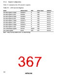
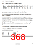
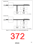
15.2.1 A/D Data Registers A to D (ADDRA to ADDRD)
Bit
15 14 13 12 11 10
9
8
7
6
—
0
5
—
0
4
—
0
3
—
0
2
—
0
1
—
0
0
—
0
ADDRn
Initial value
Read/Write
AD9 AD8 AD6 AD5 AD4 AD3 AD2 AD1 AD0
0
0
0
0
0
0
0
0
0
R
R
R
R
R
R
R
R
R
R
R
R
R
R
R
R
Bits 15 to 6—A/D Conversion Data (AD9 to AD0): 10-bit data giving an A/D conversion result.
Bits 5 to 0—Reserved: These bits cannot be modified and are always read as 0.
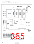
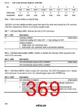
The four A/D data registers (ADDRA to ADDRD) are 16-bit read-only registers that store the
results of A/D conversion.
An A/D conversion produces 10-bit data, which is transferred for storage into the A/D data
register corresponding to the selected channel. The upper 8 bits of the result are stored in the upper
byte of the A/D data register. The lower 2 bits are stored in the lower byte. Bits 5 to 0 of an A/D
data register are reserved bits that always read 0. Table 15.3 indicates the pairings of analog input
channels and A/D data registers.
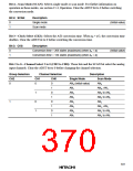
The CPU can always read the A/D data registers. The upper byte can be read directly, but the
lower byte is read through a temporary register (TEMP). For details see section 15.3, CPU
Interface.
The A/D data registers are initialized to H'0000 by a reset and in standby mode.
Table 15.3 Analog Input Channels and A/D Data Registers
Analog Input Channel
Group
AN0
0Group
AN4
1
A/D
Data
Register
ADDRA
ADDRB
ADDRC
ADDRD
AN1
AN5
AN2
AN6
AN3
AN7
339

 HITACHI [ HITACHI SEMICONDUCTOR ]