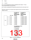
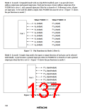
Mode 2: In mode 2 (expanded mode with on-chip ROM enabled), port 1 can provide lower
address output pins and general input pins. Each pin becomes a lower address output pin if its
P1DDR bit is set to 1, and a general input pin if this bit is cleared to 0. Following a reset, all pins
are input pins. To be used for address output, their P1DDR bits must be set to 1. Figure 7.3 shows
the pin functions in mode 2.
When P1DDR = 1
When P1DDR = 0
A7 (output)
A6 (output)
A5 (output)
A4 (output)
A3 (output)
A2 (output)
A1 (output)
A0 (output)
P17 (input)
P16 (input)
P15 (input)
P14 (input)
P13 (input)
P12 (input)
P11 (input)
P10 (input)
Port 1
Figure 7.3 Pin Functions in Mode 2 (Port 1)
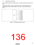
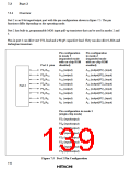
Mode 3: In mode 3 (single-chip mode), the input or output direction of each pin can be selected
individually. A pin becomes a general input pin when its P1DDR bit is cleared to 0 and a general
output pin when this bit is set to 1. Figure 7.4 shows the pin functions in mode 3.
P17 (input/output)
P16 (input/output)
P15 (input/output)
P14 (input/output)
Port 1
P13 (input/output)
P12 (input/output)
P11 (input/output)
P10 (input/output)
Figure 7.4 Pin Functions in Mode 3 (Port 1)
108

 HITACHI [ HITACHI SEMICONDUCTOR ]