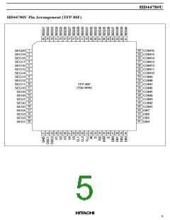
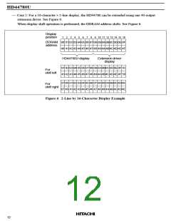
HD44780U
Function Description
Registers
The HD44780U has two 8-bit registers, an instruction register (IR) and a data register (DR).
The IR stores instruction codes, such as display clear and cursor shift, and address information for display
data RAM (DDRAM) and character generator RAM (CGRAM). The IR can only be written from the MPU.
The DR temporarily stores data to be written into DDRAM or CGRAM and temporarily stores data to be
read from DDRAM or CGRAM. Data written into the DR from the MPU is automatically written into
DDRAM or CGRAM by an internal operation. The DR is also used for data storage when reading data
from DDRAM or CGRAM. When address information is written into the IR, data is read and then stored
into the DR from DDRAM or CGRAM by an internal operation. Data transfer between the MPU is then
completed when the MPU reads the DR. After the read, data in DDRAM or CGRAM at the next address is
sent to the DR for the next read from the MPU. By the register selector (RS) signal, these two registers can
be selected (Table 1).
Busy Flag (BF)
When the busy flag is 1, the HD44780U is in the internal operation mode, and the next instruction will not
be accepted. When RS = 0 and R/W = 1 (Table 1), the busy flag is output to DB7. The next instruction
must be written after ensuring that the busy flag is 0.
Address Counter (AC)
The address counter (AC) assigns addresses to both DDRAM and CGRAM. When an address of an
instruction is written into the IR, the address information is sent from the IR to the AC. Selection of either
DDRAM or CGRAM is also determined concurrently by the instruction.
After writing into (reading from) DDRAM or CGRAM, the AC is automatically incremented by 1
(decremented by 1). The AC contents are then output to DB0 to DB6 when RS = 0 and R/W = 1 (Table 1).
Table 1
Register Selection
RS
0
R/W
Operation
0
1
0
1
IR write as an internal operation (display clear, etc.)
Read busy flag (DB7) and address counter (DB0 to DB6)
DR write as an internal operation (DR to DDRAM or CGRAM)
DR read as an internal operation (DDRAM or CGRAM to DR)
0
1
1
9

 HITACHI [ HITACHI SEMICONDUCTOR ]