ISSUED DATE :2006/08/17
REVISED DATE :
GTM
CORPORATION
Memory Organization
The internal memory organization for the GP24BC family is arranged differently for each of the densities. The
GP24BC01, for instance, is internally organized as 16 pages of 8 bytes each and requires a 7-bit data word
address. The GP24BC16, on the other hand, is organized as 128 pages of 16 bytes each with an 11-bit data
word address. The table below summarizes these differences.
Density
# of pages
16 pages
32 pages
32 pages
64 pages
128 pages
Bytes per page Data word address length
GP24BC01 (1K)
GP24BC02 (2K)
GP24BC04 (4K)
GP24BC08 (8K)
GP24BC16 (16K)
8 bytes
8 bytes
16 bytes
16 bytes
16 bytes
7 bits
8 bits
9 bits
10 bits
11 bits
PIN Capacitance
Applicable over recommended operating range from T
A=25к, f=1.0MHz, Vcc=+1.8V
Symbol
Test Condition
Max
Unit
Condition
C
I/O
Input/Output Capacitance (SDA)
Input Capacitance (A0, A1, A2, SCL)
8
6
pF
pF
V
V
I/O=0V
IN=0V
C
IN
Note: 1.This parameter is characterized and not 100% tested.
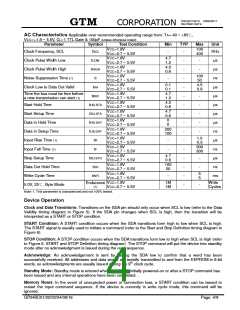
DC Characteristics
Applicable over recommended operating range from: TA=-40 ~ +85к, VCC=+1.8 ~ +5V (unless otherwise noted)
Parameter
Symbol
Test Condition
Min
TYP
Max
Unit
Supply Voltage
Supply Voltage
Supply Voltage
V
V
V
I
CC1
CC2
CC3
CC
1.8
2.7
4.5
-
-
-
-
-
-
-
-
5.5
5.5
5.5
1.0
3.0
3.0
4.0
18
5.0
5.0
CCx0.3
CC+0.5
V
V
V
Supply Current VCC=5.0V
Supply Current VCC=5.0V
Standby Current VCC=1.8V
Standby Current VCC=2.5V
Standby Current VCC=5.5V
Input Leakage Current
Output Leakage Current
Input Low Level (1)
READ at 100KHz
WRITE at 100KHz
0.4
2.0
0.6
1.4
5.0
0.2
0.1
-
mA
mA
ꢀA
ꢀA
ꢀA
ꢀA
ꢀA
V
I
CC
I
I
I
SB1
SB2
SB3
VIN= VCC or VSS
VIN= VCC or VSS
VIN= VCC or VSS
I
I
V
V
LI
LO
IL
IH
VIN= VCC or VSS
-
-
VOUT= VCC or VSS
-0.6
CCx0.7
V
V
Input High Level (1)
V
-
V
Output Low Level VCC=3.0V
Output Low Level VCC=3.0V
V
OL2
I
I
OL=2.1mA
OL=0.15mA
-
-
-
-
0.4
0.2
V
V
VOL1
Note 1: VIL and VIH max are reference only and are not tested.
GP24BC01/02/02/04/08/16
Page: 3/9

 GTM [ GTM CORPORATION ]