ISSUED DATE :2005/03/14
REVISED DATE :2006/06/01B
GTM
CORPORATION
Pin Descriptions
Name
I/O
O
I
Pin#
Function
Adj (GND)
1
Adjustable (Ground only for fixed mode)
The output of the regulator. A minimum of 10uF capacitor must be connected from this pin to
ground to insure stability.
Vout
Vin
2
The input pin of regulator. Typically a large storage capacitor is connected from this pin to ground
to insure that the input voltage does not sag below the minimum dropout voltage during the load
transient response. This pin must always be 1.4V higher than Vout in order for the device to
regulate properly.
3
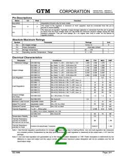
Absolute Maximum Ratings
Symbol
in
Parameter
Ratings
Unit
V
DC Supply Voltage
-0.3 to 12
V
PD
Power Dissipation
Internally Limited
ć
ć
T
ST
Storage Temperature
-65 ~ + 150
0 ~ + 150
T
OP
Operating Junction Temperature Range
Electrical Characteristics
Parameter
Conditions
MIN
TYP
1.250
1.500
1.800
2.500
3.300
5.000
-
MAX
1.275
1.530
1.836
2.550
3.365
5.100
0.2
UNIT
Reference Voltage
GE1086-Adj
GE1086-1.5
GE1086-1.8
GE1086-2.5
GE1086-3.3
GE1086-5.0
GE1086-XXX
GE1086ADJ
GE1086-1.5
GE1086-1.8
GE1086-2.5
GE1086-3.3
GE1086-5.0
Io=10mA, T
Io=10mA, T
Io=10mA, T
Io=10mA, T
Io=10mA, T
Io=10mA, T
J
J
J
J
J
J
=25к, (Vin-Vout )=1.5V
=25к, 3.0V≤Vin≤12V
=25к, 3.3V≤Vin≤12V
=25к, 4.0V≤Vin≤12V
=25к, 4.8V≤Vin≤12V
=25к, 6.5V≤Vin≤12V
1.225
V
V
1.470
1.764
V
Output Voltage
2.450
V
3.235
V
4.900
V
Line Regulator
Io=10mA, Vout+1.5<Vin<12
-
-
-
-
-
-
-
%
Vin=3.3V, 0mA<Io<1.5A, T
Vin=3.0V, 0mA<Io<1.5A, T
Vin=3.3V, 0mA<Io<1.5A, T
Vin=4.0V, 0mA<Io<1.5A, T
Vin=5.0V, 0mA<Io<1.5A, T
Vin=8.0V, 0mA<Io<1.5A, T
J
J
J
J
J
J
=25к(Note 1,2)
=25к(Note 1,2)
=25к(Note 1,2)
=25к(Note 1,2)
=25к(Note 1,2)
=25к(Note 1,2)
-
1
%
12
15
mV
mV
mV
mV
mV
15
18
Load Regulation
20
25
26
33
40
50
Dropout Voltage
(Vin-Vout)
GE1086-XXX
Io=1.5A(∆Vout=1% Vout)
-
1.3
1.4
V
Current Limit
GE1086-XXX
Vin-Vout=5V
1.6
-
5
-
A
mA
uA
Minimum Load Current Adjustable model
Vin=5V
-
-
-
-
10
Adjust Pin Current
Quiescent Current
Thermal Regulation
Adjustable model
fixed model
Vin=12V, Io=10mA
Vin=12V, Io=0mA
55
-
100
12
mA
%/W
T
A
=25к, 30ms pulse
0.008
0.04
F=120Hz, COUT=25uF, Tantalum, Io=1.5A
GE1086-XXX
Io=10mA
Vin=Vout+3V
-
-
60
70
-
dB
%
Temperature Stability
0.5
Thermal Resistance
Junction-to-Ambient
(No heat sink ;No air flow)
-
86
-
-
к/W
к/W
Thermal Resistance
Junction-to-Case
Control Circuitry/Power Transistor
-
0.65/2.7
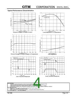
Note 1: See thermal regulation specifications for changes in output voltage due to heating effects. Line and load regulation are measured
at a constant junction Temperature by low duty cycle pulse testing. Load regulation is measured at the output lead =1/18” from the
package.
Note 2: Line and load regulation are guaranteed up to the maximum power dissipation of 15W. Power dissipation is determined by the
difference in input and output and the output current. Guaranteed maximum power dissipation will not be available over the full
input/output range.
GE1086
Page: 2/4

 GTM [ GTM CORPORATION ]