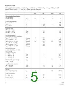
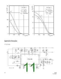
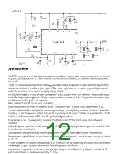
• TCA440 T
+V
CC
100n
+50%
-20%
W
47µ ±50%
Rp2
1.5n
±2.5%
W
1.5k
±2%
S2
10n
+50%
-20%
16
10
12
15
4
14
7
S3
W1a
100n
+50%
-20%
330p
±2.5%
5
6
4.7µ
A
x
W1
±50%
TCA 440 T
R
2
1
Rp3
W
3.3n
12k
~
~
~
+50%
-20%
±2%
V
AF
1.5n
V
±2.5%
goHF
3
8
11
13
9
1.8k
100 ±2%
39k ±2%
±2%
S1
100n
8.2k
+50%
-20%
100n
+50%
-20%
±5%
20µ
25Ω ≤ RG ≤
100Ω
±20%
4.7µ
±50%
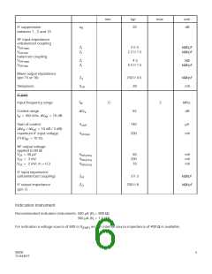
Application Hints
The PCB is to arrange such that there are maximum ground lines (ground area) voltage supply has to be blocked
to ground by a capacitor of 10...100 nF in order to avoid distortions. Blocking should be as close as possible to
the circuit.
The RF circuit has to layout such that 150 mV
oscillator voltage are applied to pin 5. Symmetrically applying
(rms)
an external oscillator is possible to pin 4 or pin 5. The unused input must be connected to ground via capacitor
and in the same time be connected to supply voltage at pin 6.
It is recommendable to profide off earth connections 1 and 3, because in this way common - mode interferences
more effectively can be suppessed. Single - sided capacitive control of pin 1 and 2 is possible, the unused input
must be connected to ground via capacitor.
Mixer outputs 15 and 16 can be used equivalently.
Load resistances of the mixer (IF selection) at pin 15 respectively pin 16 should run to approximately 7 kΩ.
To avoid saturation of the multiplier the maximum peak voltage occuring during operation should not exceed the
level (V - 3 V) IF response to voltage from pin 15 respectively pin 16 to pin 12 should be approximately - 18 dB
CC
that the control characteristics of IF - and RF - part optimally be matched.
Peak voltage at pin 7 occuring during operation should not exceed 2 V that the IF output does not go into
saturation.
All the RF bypass capacitors should amount to 100 nF. Sufficient decoupling of wavemagnet and oscillator coil is
to be taken into consideration.
All components and parts must be carefully proportioned in order to obtain optimum wise characteristics.
Wavemagnets applied should so much mass as possible. The transformation ratio of the input circuitry should run
to 10...12.
In order to improve RF response characteristic a RF preselector can be additionally preceded or the wavemagnet
can be tighty coupled by means of an emitter follower impedance transformer.
Improvement of signal - to - noise ratio at average input voltages can be obtained by delayed control of the RF
part. Control should be start at approximately 1...2 mV.

 GSG [ GUNTER SENICONDUCTOR GMBH. ]