Global Mixed-mode Technology Inc.
G940/G941
Absolute Maximum Ratings
(Note 1)
Operating Conditions
(Note 1)
Input Voltage……………………………..……..…..…10V
Input Voltage………………………….…………….4V~7V
Temperature Range………………….…0°C ≤ TJ ≤125°C
Power Dissipation Internally Limited
..(Note 2)
Maximum Junction Temperature………….….…...150°C
Storage Temperature Range…..…..…..-65°C ≤ TJ ≤+150°C
Lead Temperature, Time for Wave Soldering
SOT 89, SOT23 Package….….…..……..…....260°C, 4s
Continuous Power Dissipation (TA = + 25°C)
SOT 23(1)…….…………………….….……….……...0.3W
SOT 89(1)……………………….………..………..…0.42W
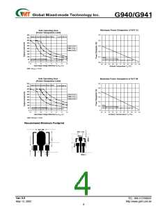
Note (1): See Recommended Minimum Footprint.
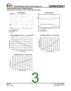
Electrical Characteristics
VIN =5V, IO = 400mA, CIN = 1 µF, COUT =10 µF, All specifications apply for TA = TJ = 25°C. [Note 3]
PARAMETER
CONDITIONS
MIN
TYP
-
0.08
-
100
0.6
42
0.8
130
0.76
125
MAX
UNITS
%
%/V
%
mΩ
mA
dB
V
mV
A
°C
Output Voltage Accuracy IO = 10mA
-2
-
+3
0.9
2.2
-
Line Regulation
Load Regulation
Output Impedance
Quiescent Current
Ripple Rejection
Dropout Voltage
VIN = 4V to 7V, IO = 50mA
IO = 10mA to 400mA
100mA DC and 100mA AC, fo = 120Hz
VIN=5V
-
-
-
-
-
-
-
-
-
-
fi = 120 Hz, 1VP-P, Io = 100mA
IO = 400mA
IO = 100mA
0.9
150
-
Short Circuit Current
Over Temperature
-
Note 1:
Note2:
Absolute Maximum Ratings are limits beyond which damage to the device may occur. Operating Condi-
tions are conditions under which the device functions but the specifications might not be guaranteed. For
guaranteed specifications and test conditions see the Electrical Characteristics.
The maximum power dissipation is a function of the maximum junction temperature, TJmax ; total thermal re-
sistance, θJA, and ambient temperature TA. The maximum allowable power dissipation at any ambient tem-
perature is Tjmax-TA / θJA. If this dissipation is exceeded, the die temperature will rise above 130°C and IC
will go into thermal shutdown. For the G940/G941 in SOT 23 package, θJA is 350°C/W and in the SOT 89
package is 250°C/W (See Recommend Minimum Footprint). The safe operation in SOT 23 & SOT 89
package, it can see “Typical Performance Characteristics” (Safe Operating Area).
Note3:
Note4:
Low duty pulse techniques are used during test to maintain junction temperature as close to ambient as
possible.
The type of output capacitor should be tantalum or aluminum.
Load Regulation
Definitions
The change in output voltage for a change in load
current at constant chip temperature. The measure-
ment is made under conditions of low dissipation or by
using pulse techniques such that average chip tem-
perature is not significantly affected.
Dropout Voltage
The input/output Voltage differential at which the
regulator output no longer maintains regulation against
further reductions in input voltage. Measured when the
output drops 100mV below its nominal value, dropout
voltage is affected by junction temperature, load cur-
rent and minimum input supply requirements.
Maximum Power Dissipation
The maximum total device dissipation for which the
regulator will operate within specifications.
Line Regulation
The change in output voltage for a change in input
voltage. The measurement is made under conditions
of low dissipation or by using pulse techniques such
that average chip temperature is not significantly af-
fected.
Quiescent Bias Current
Current which is used to operate the regulator chip
and is not delivered to the load.
Ver: 5.5
May 13, 2002
TEL: 886-3-5788833
http://www.gmt.com.tw
2

 GMT [ GLOBAL MIXED-MODE TECHNOLOGY INC ]