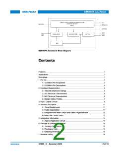
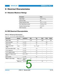
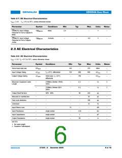
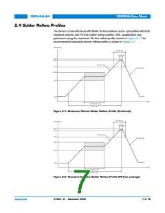
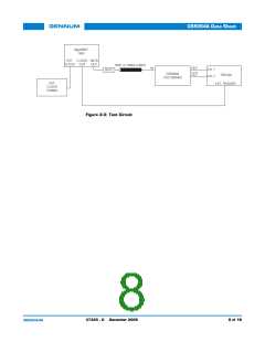
GS9064A Data Sheet
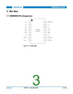
1.2 GS9064A Pin Descriptions
Table 1-1: GS9064A Pin Descriptions
Pin Number
Name
Timing
Type
Description
1
CLI
Analog
Output
Cable Length Indicator.
An analog voltage will be output proportional to the cable length
connected to the serial digital input.
2, 15
VCC
Analog
Analog
Power
Power
Most positive power supply connection.
Connect to +3.3V DC.
3, 6, 11, 14
VEE
Most negative power supply connection.
Connect to GND.
4, 5
7, 8
SDI, SDI
Analog
Analog
Input
–
Serial digital differential input.
AGC+,
AGC-
External AGC capacitor.
Connect pin 7 and pin 8 together through a 1uF capacitor.
9
BYPASS
MCLADJ
Not
Synchronous
Input
Input
Forces the Equalizing and DC RESTORE stages into bypass mode
when HIGH. No equalization occurs in this mode.
10
Analog
Maximum cable length adjust.
Adjusts the approximate maximum amount of cable to be equalized
(from 0m to the maximum cable length). The output is muted (latched to
the last state) when the maximum cable length is achieved.
12, 13
16
SDO, SDO
CD/MUTE
Analog
Output
Equalized serial digital differential output.
Not
Synchronous
Bidirectional
STATUS SIGNAL OUTPUT / CONTROL SIGNAL INPUT
levels are LVCMOS/LVTTL compatible.
OUTPUT (CD):
Indicates the presence of a valid input signal. When the CD pin is LOW,
a valid input signal has been detected. When this pin is HIGH, the input
signal is invalid. If CD is set HIGH, the serial digital output of the device
will be forced to a steady state (latched to the last state).
NOTE: This pin will indicate loss of carrier for data rates > 19Mb/s.
INPUT (MUTE):
When the MUTE pin is set HIGH by the application interface, the serial
digital output of the device will be forced to a steady state (latched to the
last state). When the MUTE pin is set LOW, the serial digital output of
the device will be active.
NOTE: The CD/MUTE pin is not functional when BYPASS is set HIGH.
37325 - 0 December 2005
4 of 16

 GENNUM [ GENNUM CORPORATION ]