GS9064A Data Sheet
4. Detailed Description
The GS9064A is a high speed BiCMOS IC designed to equalize serial digital
signals.
The GS9064A can equalize both HD and SD serial digital signals, and will typically
equalize greater than 350m at 270Mb/s.
The GS9064A/ is powered from a single +3.3V power supply and consumes
approximately 265mW of power.
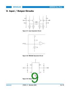
4.1 Serial Digital Inputs
The serial data signal may be connected to the input pins (SDI/SDI) in either a
differential or single ended configuration. AC coupling of the inputs is
recommended, as the SDI and SDI inputs are internally biased at approximately
1.8V.
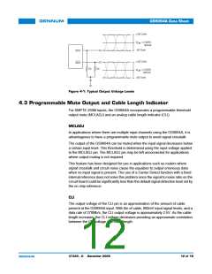
4.2 Cable Equalization
The input signal passes through a variable gain equalizing stage whose frequency
response closely matches the inverse of the cable loss characteristic. In addition,
the variation of the frequency response with control voltage imitates the variation
of the inverse cable loss characteristic with cable length.
The edge energy of the equalized signal is monitored by a detector circuit which
produces an error signal corresponding to the difference between the desired edge
energy and the actual edge energy. This error signal is integrated by both an
internal and an external AGC filter capacitor providing a steady control voltage for
the gain stage. As the frequency response of the gain stage is automatically varied
by the application of negative feedback, the edge energy of the equalized signal is
kept at a constant level which is representative of the original edge energy at the
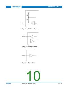
transmitter. The equalized signal is also DC restored, effectively restoring the logic
threshold of the equalized signal to its correct level independent of shifts due to AC
coupling. The digital output signals have a nominal voltage of 750mV differential,
pp
or 375mV single ended when terminated with 50Ω as shown in Figure 4-1.
pp
37325 - 0 December 2005
11 of 16

 GENNUM [ GENNUM CORPORATION ]