MB3771
■ FUNCTIONAL DESCRIPTIONS
Comparators Comp.A and Comp.B apply a hysteresis to the detected voltage, so that when the voltage at either
the VSA or VSB pin falls below 1.23 V the RESET output signal goes to “low” level.
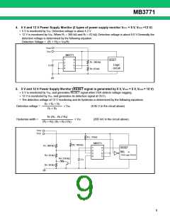
Comp. B may be used to detect any given voltage(Sample Application 3), and can also be used as a forced
reset pin (with reset hold time) with TTL input (Sample Application 6).
Note that if Comp.B is not used, the VSB pin should be connected to the VCC pin (Sample Application 1).
Instantaneous breaks or drops in the power supply can be detected as abnormal conditions by the MB3771
within a 2 µs interval. However because momentary breaks or drops of this duration do not cause problems in
actual systems in some cases, a delayed trigger function can be created by connecting capacitors to the VSA or
VSB pin (Sample Application 8).
Because the RESET output has built-in pull-up resistance, there is no need to connect to external pull-up
resistance when connected to a high impedance load such as a CMOS logic IC.
Comparator Comp. C is an open-collector output comparator without hysteresis, in which the polarity of input/
output characteristics is reversed. Thus Comp. C is useful for over-voltage detection (Sample Application 11)
and positive logic RESET signal output (Sample Application 7), as well as for creating a reference voltage
(Sample Application 10).
Note that if Comp. C is not used, the VSC pin should be connected to the GND pin (Sample Application 1).
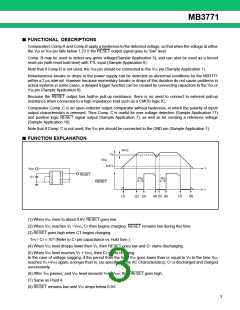
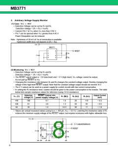
■ FUNCTION EXPLANATION
VHYS
VS
VCC
0.8 V
t
t
VCC
CT
1
2
3
4
8
7
6
5
RESET
TPO
TPO
RESET
(1)
(2) (3)
(4) (5) (6)
(7)
(8)
(1) When VCC rises to about 0.8V, RESET goes low.
(2) When VCC reaches VS +VHYS, CT then begins charging. RESET remains low during this time
(3) RESET goes high when CT begins charging.
TPO =: CT × 10 5 (Refer to CT pin capacitance vs. hold time )
(4) When VCC level dropps lower then VS, then RESET goes low and CT starts discharging.
(5) When VCC level reaches VS + VHYS, then CT starts charging.
In the case of voltage sagging, if the period from the time VCC goes lower than or equal to VS to the time VCC
reaches VS +VHYS again, is longer than tPI, (as specified in the AC Characteristics), CT is discharged and charged
successively.
(6) After TPO passes, and VCC level exceeds VS + VHYS, then RESET goes high.
(7) Same as Point 4.
(8) RESET remains low until VCC drops below 0.8V.
3

 FUJITSU [ FUJITSU ]