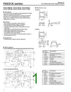
FA531X series
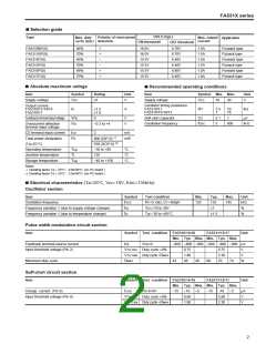
■ Selection guide
UVLO (typ.)
Type
Polarity of overcurrent
detection
Max. duty
cycle (typ.)
Max. output
current
Application
ON threshold
OFF threshold
FA5310BP(S)
FA5311BP(S)
FA5314P(S)
FA5315P(S)
FA5316P(S)
FA5317P(S)
46%
70%
46%
70%
46%
70%
+
+
–
–
+
+
16.0V
16.0V
15.5V
15.5V
15.5V
15.5V
8.70V
8.70V
8.40V
8.40V
8.40V
8.40V
1.5A
1.5A
1.5A
1.5A
1.0A
1.0A
Forward type
Flyback type
Forward type
Flyback type
Forward type
Flyback type
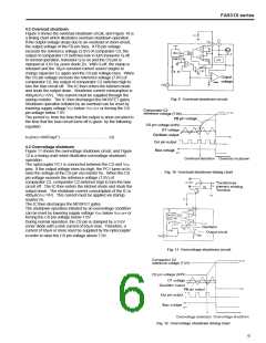
■ Absolute maximum ratings
■ Recommended operating conditions
Item
Symbol Min. Max.
Unit
Item
Symbol
Rating
Unit
Supply voltage
VCC
10
30
V
Supply voltage
VCC
31
V
Oscillator timing resistance
FA5310/11
FA5314/15/16/17
Output current
FA5310/11/14/15
FA5316/17
RT
3.3
1
10
10
kΩ
IO
±1.5
±1.0
A
Soft-start capacitor
CS
0.1
5
1
µF
Feedback terminal input voltage
VFB
VIS
4
V
V
Oscillation frequency
fOSC
600
kHz
Overcurrent detection
terminal input voltage
–0.3 to +4
CS terminal input current
Total power dissipation
(Ta=25°C)
ICS
Pd
2
mA
800 (DIP-8) *1
550 (SOP-8) *2
–30 to +85
125
mW
Operating temperature
Junction temperature
Storage temperature
Notes:
Topr
Tj
°C
°C
°C
Tstg
–40 to +150
1 Derating factor Ta > 25°C : 8.0mW/°C (on PC board )
2 Derating factor Ta > 25°C : 5.5mW/°C (on PC board )
*
*
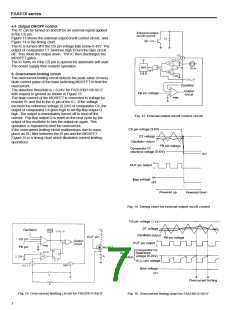
■ Electrical characteristics (Ta=25°C, Vcc=18V, fOSC=135kHz)
Oscillator section
Item
Symbol
fOSC
fdV
Test condition
Min.
125
Typ.
Max.
Unit
Oscillation frequency
RT=5.1kΩ, CT=360pF
VCC=10 to 30V
135
±1
145
kHz
%
Frequency variation 1 (due to supply voltage change)
Frequency variation 1 (due to temperature change)
fdr
Ta=–30 to +85°C
±1.5
%
Pulse width modulation circuit section
Item
Symbol Test condition FA5310/14/16
Min. Typ. Max. Min. Typ. Max.
–660 –800 –960 –660 –800 –960 µA
FA5311/15/17
Unit
Feedback terminal source current
Input threshold voltage (Pin 2)
IFB
VFB=0
VTH FBO Duty cycle =0%
VTH FBM Duty cycle =DMAX
DMAX
0.75
1.80
46
0.75
2.30
70
V
V
Maximum duty cycle
43
49
66
74
%
Soft-start circuit section
Item
Symbol Test condition FA5310/14/16
FA5311/15/17
Unit
Min. Typ. Max. Min. Typ. Max.
Charge current (Pin 8)
ICHG
Pin 8=0V
–15
–10
–5
–15
–10
–5
µA
V
Input threshold voltage (Pin 8)
VTH CSO Duty cycle =0%
VTH CSM Duty cycle =DMAX
0.90
1.90
0.90
2.30
V
2

 FUJI [ FUJI ELECTRIC ]