Page 5
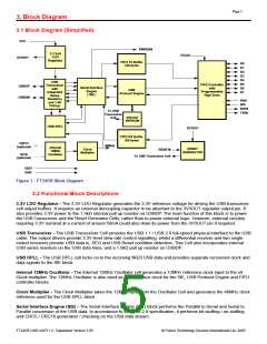
3. Block Diagram
3.1 Block Diagram (Simplified)
VCC
PWREN#
3.3 Volt
LDO
VCCIO
3V3OUT
Regulator
FIFO TX Buffer
128 bytes
D0
D1
D2
D3
D4
D5
D6
D7
USB
Transceiver
with
Integrated
Series
Resistors
and 1.5K
Pull-up
FIFO Controller
with
Programmable
High Drive
USBDP
USBDM
Serial Interface
Engine
USB
Protocol Engine
( SIE )
RD#
WR
RXF#
TXE#
To USB
Transceiver
Cell
Internal
EEPROM
USB DPLL
3V3OUT
FIFO RX Buffer
256 bytes
OSCO
(optional)
48MHz
Internal
12MHz
Oscillator
RESET
GENERATOR
Clock
Multiplier
RESET#
To USB Transceiver Cell
OCSI
(optional)
TEST
GND
Figure 1 - FT245R Block Diagram
3.2 Functional Block Descriptions
3.3V LDO Regulator - The 3.3V LDO Regulator generates the 3.3V reference voltage for driving the USB transceiver
cell output buffers. It requires an external decoupling capacitor to be attached to the 3V3OUT regulator output pin. It
also provides 3.3V power to the 1.5kΩ internal pull up resistor on USBDP. The main function of this block is to power
the USB Transceiver and the Reset Generator Cells, rather than to power external logic. However, external circuitry
requiring 3.3V nominal at a current of around 50mA could also draw its power from the 3V3OUT pin if required.
USB Transceiver - The USB Transceiver Cell provides the USB 1.1 / USB 2.0 full-speed physical interface to the USB
cable. The output drivers provide 3.3V level slew rate control signalling, whilst a differential receiver and two single
ended receivers provide USB data in, SEO and USB Reset condition detection. This Cell also incorporates internal
USB series resistors on the USB data lines, and a 1.5kΩ pull up resistor on USBDP.
USB DPLL - The USB DPLL cell locks on to the incoming NRZI USB data and provides separate recovered clock and
data signals to the SIE block.
Internal 12MHz Oscillator - The Internal 12MHz Oscillator cell generates a 12MHz reference clock input to the x4
Clock multiplier. The 12MHz Oscillator is also used as the reference clock for the SIE, USB Protocol Engine and FIFO
controller blocks
Clock Multiplier - The Clock Multiplier takes the 12MHz input from the Oscillator Cell and generates the 48MHz clock
reference used for the USB DPLL block.
Serial Interface Engine (SIE) - The Serial Interface Engine (SIE) block performs the Parallel to Serial and Serial to
Parallel conversion of the USB data. In accordance to the USB 2.0 specification, it performs bit stuffing / un-stuffing
and CRC5 / CRC16 generation / checking on the USB data stream.
FT245R USB UART I.C. Datasheet Version 1.05
© Future Technology Devices International Ltd. 2005

 FTDI [ FUTURE TECHNOLOGY DEVICES INTERNATIONAL LTD. ]