Document No.: FT_000288
FT232H SINGLE CHANNEL HI-SPEED USB TO MULTIPURPOSE UART/FIFO IC
Datasheet Version 1.82
Clearance No.: FTDI #199
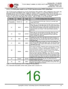
3.5.2 FT232H pins used in an FT245 Synchronous FIFO Interface
The FT232H can be configured as a FT245 synchronous FIFO interface. When configured in this mode, the
pins used and the descriptions of the signals are shown in Table 3.7. To set this mode the external
EEPROM must be set to 245 modes. A software command (FT_SetBitMode) is then sent by the application
to the FTDI D2xx driver to tell the chip to enter 245 synchronous FIFO mode. In this mode, data is
written or read on the rising edge of the CLKOUT. Refer to Figure 4.4 for timing details.
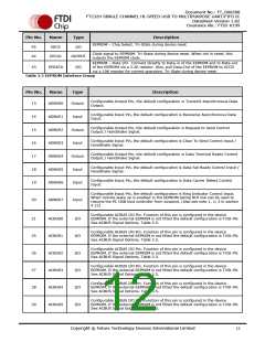
Pin No.
Name
Type
FT245 Configuration Description
13,14,15,16,
17,18,19,20
D7 to D0 bidirectional FIFO data. This bus is normally input
unless OE# is low.
ADBUS[7:0]
I/O
When high, do not read data from the FIFO. When low, there
is data available in the FIFO which can be read by driving RD#
low. When in synchronous mode, data is transferred on every
clock that RXF# and RD# are both low. Note that the OE# pin
must be driven low at least 1 clock period before asserting
RD# low.
21
25
RXF#
TXE#
OUTPUT
OUTPUT
When high, do not write data into the FIFO. When low, data
can be written into the FIFO by driving WR# low. When in
synchronous mode, data is transferred on every clock that
TXE# and WR# are both low.
Enables the current FIFO data byte to be driven onto D0...D7
when RD# goes low. The next FIFO data byte (if available) is
fetched from the receive FIFO buffer each CLKOUT cycle until
RD# goes high.
Enables the data byte on the D0...D7 pins to be written into
the transmit FIFO buffer when WR# is low. The next FIFO data
byte is written to the transmit FIFO buffer each CLKOUT cycle
until WR# goes high.
26
27
RD#
WR#
INPUT
INPUT
The Send Immediate / WakeUp signal combines two functions
on a single pin. If USB is in suspend mode (PWREN# = 1) and
remote wakeup is enabled in the EEPROM, strobing this pin
low will cause the device to request a resume on the USB Bus.
Normally, this can be used to wake up the Host PC.
28
SIWU#
INPUT
During normal operation (PWREN# = 0), if this pin is strobed
low any data in the device RX buffer will be sent out over USB
on the next Bulk-IN request from the drivers regardless of the
pending packet size. This can be used to optimize USB transfer
speed for some applications. Tie this pin to VCCIO if not used.
60 MHz Clock driven from the chip. All signals should be
synchronized to this clock.
29
30
CLKOUT
OE#
OUTPUT
INPUT
Output enable when low to drive data onto D0-7. This should
be driven low at least 1 clock period before driving RD# low to
allow for data buffer turn-around.
Table 3.7 FT245 Synchronous FIFO Configured Pin Descriptions
For a functional description of this mode, please refer to section 4.4
Copyright © Future Technology Devices International Limited
16

 FTDI [ FUTURE TECHNOLOGY DEVICES INTERNATIONAL LTD. ]