Order this document
by MSD6150/D
SEMICONDUCTOR TECHNICAL DATA
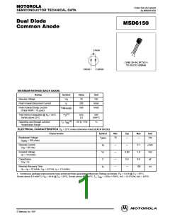
3 Anode
1
2
3
CASE 29–04, STYLE 4
TO–92 (TO–226AA)
Cathode 1
2 Cathode
MAXIMUM RATINGS (EACH DIODE)
Rating
Reverse Voltage
Symbol
Value
Unit
Vdc
V
R
70
Peak Forward Recurrent Current
I
200
500
mAdc
mAdc
F
Peak Forward Surge Current
(Pulse Width = 10 µsec)
I
FM(surge)
(1)
Total Device Dissipation @ T = 25°C
Derate above 25°C
P
D
625
5.0
mW
mW/°C
A
(1)
T , T
J stg
Operating and Storage Junction
Temperature Range
–55 to +135
°C
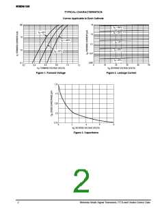
ELECTRICAL CHARACTERISTICS (T = 25°C unless otherwise noted) (EACH DIODE)
A
Characteristic
Symbol
Min
Typ
Max
Unit
Breakdown Voltage
(I = 100 µAdc)
V
70
—
—
Vdc
(BR)
(BR)
Reverse Current
I
R
—
—
—
—
—
0.80
5.0
—
0.1
1.0
8.0
100
µAdc
Vdc
pF
(V = 50 Vdc)
R
Forward Voltage
(I = 10 mAdc)
F
V
F
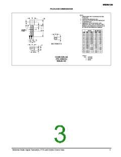
Capacitance
(V = 0)
R
C
Reverse Recovery Time
t
rr
ns
(I = I = 10 mAdc, V = 5.0 Vdc, i = 1.0 mAdc)
rr
F
R
R
1. Continuous package improvements have enhanced these guaranteed Maximum Ratings as follows: P = 1.0 W @ T = 25°C,
D
C
Derate above 8.0 mW/°C, P = 10 W @ T = 25°C, Derate above 80 mW/°C, T , T = –55 to +150°C, θJC = 12.5°C/W, θJA = 125°C.
D
C
J
stg
Motorola Small–Signal Transistors, FETs and Diodes Device Data
Motorola, Inc. 1997
1

 FREESCALE [ Freescale ]