FUNCTIONAL DESCRIPTION
FUNCTIONAL INTERNAL BLOCK DESCRIPTION
FUNCTIONAL INTERNAL BLOCK DESCRIPTION
Figure 4. Functional Internal Block Diagram
with the corresponding SPI input data register contents. All
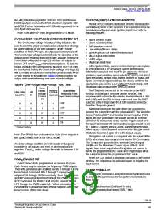
POWER SUPPLY/POR
outputs are disabled when the OUTEN pin is HIGH,
regardless of the state of the command inputs.
The 33810 is designed to operate from 4.5 to 36 V on the
VPWR pin. The VPWR pin supplies power to all internal
regulators, analog, and logic circuit blocks. The VDD supply
is used for setting communication threshold levels and
supplying power to the SO driver. This IC architecture
provides a low quiescent current sleep mode. Applying
VPWR and VDD to the device will generate a Power On
Reset (POR) and place the device in the Normal State. The
Power On Reset circuit incorporates a timer to prevent high
frequency transients from causing a POR.
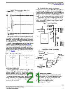
INJECTOR DRIVERS: OUT0 – OUT3
These pins are the Open drain low side (Injector) driver
outputs. The drain voltage is actively clamped during turn off
of inductive loads. These outputs can be connected in
parallel for higher current loads, provided the turn off energy
rating is not exceeded.
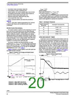
IGNITION GATE PRE-DRIVERS: GD0 – GD3
MCU INTERFACE AND OUTPUT CONTROL
These pins are the gate drive outputs for an external
MOSFET or IGBT. Internal to the device is a Gate to Source
resistor designed to hold the external device in the OFF state
while the device is in the POR or Sleep State.
This component provides parallel input pins for OUT0-
OUT3 low side drivers and GD0-GD3 gate drivers. Each
parallel input control pin is active high and has an internal
pulldown current sink. The parallel input data is logically OR’d
33810
Analog Integrated Circuit Device Data
Freescale Semiconductor
17

 FREESCALE [ Freescale ]