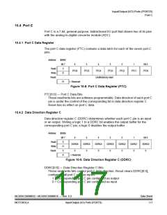
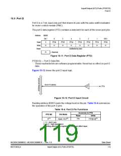
Input/Output (I/O) Ports (PORTS)
Port E
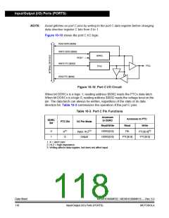
NOTE:
Avoid glitches on port E pins by writing to the port E data register before changing
data direction register E bits from 0 to 1.
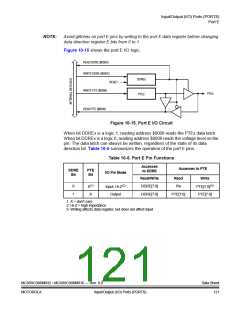
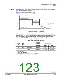
Figure 10-15 shows the port E I/O logic.
READ DDRE ($000C)
WRITE DDRE ($000C)
DDREx
RESET
WRITE PTE ($0008)
PTEx
PTEx
READ PTE ($0008)
Figure 10-15. Port E I/O Circuit
When bit DDREx is a logic 1, reading address $0008 reads the PTEx data latch.
When bit DDREx is a logic 0, reading address $0008 reads the voltage level on the
pin. The data latch can always be written, regardless of the state of its data
direction bit. Table 10-5 summarizes the operation of the port E pins.
Table 10-5. Port E Pin Functions
Accesses
Accesses to PTE
DDRE
Bit
PTE
Bit
to DDRE
Read/Write
DDRE[7:0]
DDRE[7:0]
I/O Pin Mode
Read
Pin
Write
X(1)
X
Input, Hi-Z(2)
Output
PTE[7:0](3)
PTE[7:0]
0
1
PTE[7:0]
1. X = don’t care
2. Hi-Z = high impedance
3. Writing affects data register, but does not affect input.
MC68HC908MR32 • MC68HC908MR16 — Rev. 6.0
MOTOROLA Input/Output (I/O) Ports (PORTS)
Data Sheet
121

 FREESCALE [ Freescale ]