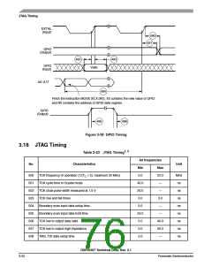
JTAG Timing
EXTAL
(Input)
490
491
GPIO
(Output)
492
493
GPIO
(Input)
Valid
A0–A17
494
Fetch the instruction MOVE X0,X:(R0); X0 contains the new value of GPIO
and R0 contains the address of GPIO data register.
GPIO
(Output)
495
496
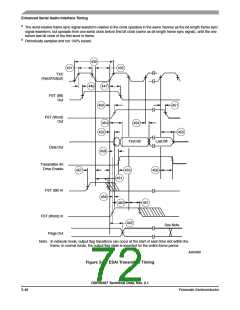
Figure 3-38 GPIO Timing
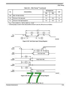
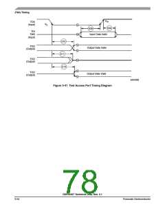
3.18 JTAG Timing
Table 3-23 JTAG Timing1, 2
All frequencies
Min Max
No.
Characteristics
Unit
500
501
502
503
504
505
506
507
508
TCK frequency of operation (1/(TC × 3); maximum 22 MHz)
TCK cycle time in Crystal mode
0.0
45.0
20.0
0.0
22.0
—
MHz
ns
TCK clock pulse width measured at 1.5 V
TCK rise and fall times
—
ns
3.0
—
ns
Boundary scan input data setup time
Boundary scan input data hold time
TCK low to output data valid
5.0
ns
24.0
0.0
—
ns
40.0
40.0
—
ns
TCK low to output high impedance
TMS, TDI data setup time
0.0
ns
5.0
ns
DSP56367 Technical Data, Rev. 2.1
3-52
Freescale Semiconductor

 FREESCALE [ Freescale ]