Freescale Semiconductor, Inc.
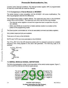
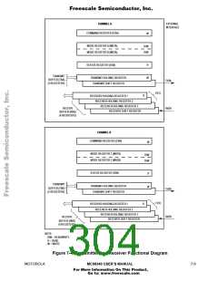
ADDRESS BUS
CONTROL
X1
X2
INTERNAL
CONTROL
LOGIC
BAUD RATE
GENERATOR
LOGIC
SCLK
S
E
R
I
A
L
DATA
D7–D0
CHANNEL A
DATA BUS
D15–D0
DATA BUS
MUX
M
O
D
U
L
FOUR-CHARACTER
RECEIVE BUFFER
RxDA
TxDA
TWO-CHARACTER
TRANSMIT BUFFER
E
RTSA
CTSA
I
N
T
E
R
N
A
L
TxRDYA
..... ....
.
CHANNEL B
FOUR-CHARACTER
RECEIVE BUFFER
RxDB
TxDB
B
U
S
TWO-CHARACTER
TRANSMIT BUFFER
RTSB
CTSB
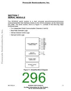
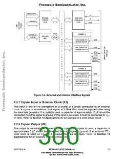
Figure 7-2. External and Internal Interface Signals
7.2.1 Crystal Input or External Clock (X1)
This input is one of two connections to a crystal or a single connection to an external
clock. A crystal or an external clock signal, at 3.6864 MHz, must be supplied when using
the baud rate generator. If a crystal is used, a capacitor of approximately 10 pF should be
connected from this signal to ground. If this input is not used, it must be connected to V
CC
or GND. Refer to Section 10 Applications for an example of a clock driver circuit.
7.2.2 Crystal Output (X2)
This output is the additional connection to a crystal. If a crystal is used, a capacitor of
approximately 5 pF should be connected from this signal to ground. If an external TTL-
level clock is used on X1, the X2 output must be left open. Refer to Section 10
Applications for an example of a clock driver circuit.
MOTOROLA
MC68340 USER’S MANUAL
7- 5
For More Information On This Product,
Go to: www.freescale.com

 FREESCALE [ Freescale ]