Freescale Semiconductor, Inc.
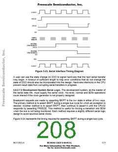
The serial interface uses a full-duplex synchronous protocol similar to the serial peripheral
interface (SPI) protocol. The development system serves as the master of the serial link
since it is responsible for the generation of DSCLK. If DSCLK is derived from the CPU32
system clock, development system serial logic is unhindered by the operating frequency of
the target processor. Operable frequency range of the serial clock is from DC to one-half
the processor system clock frequency.
The serial interface operates in full-duplex mode—i.e., data is transmitted and received
simultaneously by both master and slave devices. In general, data transitions occur on the
falling edge of DSCLK and are stable by the following rising edge of DSCLK. Data is
transmitted MSB first and is latched on the rising edge of DSCLK.
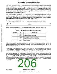
The serial data word is 17 bits wide—16 data bits and a status/control (S/C) bit.
16
15
0
S/C
DATA FIELD
Bit 16 indicates the status of CPU-generated messages as shown in Table 5-21.
Table 5-21. CPU Generated Message Encoding
Encoding
Data
xxxx
Message Type
Valid Data Transfer
0
0
1
1
1
Command Complete; Status OK
Not Ready with Response; Come Again
BERR Terminated Bus Cycle; Data Invalid
Illegal Command
FFFF
0000
0001
FFFF
Command and data transfers initiated by the development system should clear bit 16. The
current implementation ignores this bit; however, Motorola reserves the right to use this bit
for future enhancements.
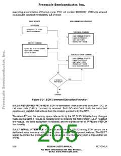
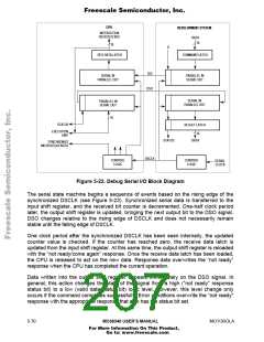
5.6.2.7.1 CPU Serial Logic. CPU serial logic, shown in the left-hand portion of Figure 5-
22, consists of transmit and receive shift registers and of control logic that includes
synchronization, serial clock generation circuitry, and a received bit counter.
Both DSCLK and DSI are synchronized to on-chip clocks, thereby minimizing the chance
of propagating metastable states into the serial state machine. Data is sampled during the
high phase of CLKOUT. At the falling edge of CLKOUT, the sampled value is made
available to internal logic. If there is no synchronization between CPU32 and development
system hardware, the minimum hold time on DSI with respect to DSCLK is one full period
of CLKOUT.
MOTOROLA
MC68340 USER’S MANUAL
5- 69
For More Information On This Product,
Go to: www.freescale.com

 FREESCALE [ Freescale ]