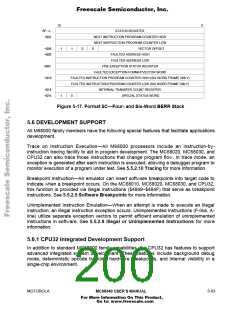
Freescale Semiconductor, Inc.
The CPU writes a unique value indicating the source of BDM transition into temporary
register A (ATEMP) as part of the process of entering BDM. A user can poll ATEMP and
determine the source (see Table 5-20) by issuing a read system register command
(RSREG). ATEMP is used in most debugger commands for temporary storage—it is
imperative that the RSREG command be the first command issued after transition into
BDM.
Table 5-20. Polling the BDM Entry Source
Source
ATEMP 31–16
SSW*
ATEMP 15–0
$FFFF
Double Bus Fault
BGND Instruction
Hardware Breakpoint
$0000
$0001
$0000
$0000
*SSW is described in detail in 5.5.3 Fault Recovery.
A double bus fault during initial SP/PC fetch sequence is distinguished by a value of
$FFFFFFFF in the current instruction PC. At no other time will the processor write an odd
value into this register.
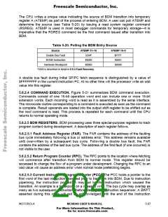
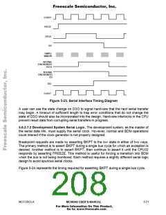
5.6.2.4 COMMAND EXECUTION. Figure 5-21 summarizes BDM command execution.
Commands consist of one 16-bit operation word and can include one or more 16-bit
extension words. Each incoming word is read as it is assembled by the serial interface.
The microcode routine corresponding to a command is executed as soon as the command
is complete. Result operands are loaded into the output shift register to be shifted out as
the next command is read. This process is repeated for each command until the CPU
returns to normal operating mode.
5.6.2.5 BDM REGISTERS. BDM processing uses three special-purpose registers to track
program context during development. A description of each register follows.
5.6.2.5.1 Fault Address Register (FAR). The FAR contains the address of the faulting
bus cycle immediately following a bus or address error. This address remains available
until overwritten by a subsequent bus cycle. Following a double bus fault, the FAR
contains the address of the last bus cycle. The address of the first fault (if one occurred) is
not visible to the user.
5.6.2.5.2 Return Program Counter (RPC). The RPC points to the location where fetching
will commence after transition from BDM to normal mode. This register should be
accessed to change the flow of a program under development. Changing the RPC to an
odd value will cause an address error when normal mode prefetching begins.
5.6.2.5.3 Current Instruction Program Counter (PCC). The PCC holds a pointer to the
first word of the last instruction executed prior to transition into BDM. Due to instruction
pipelining, the instruction pointed to may not be the instruction which caused the
transition. An example is a breakpoint on a released write. The bus cycle may overlap as
many as two subsequent instructions before stalling the instruction sequencer. A BKPT
asserted during this cycle will not be acknowledged until the end of the instruction
MOTOROLA
MC68340 USER’S MANUAL
5- 67
For More Information On This Product,
Go to: www.freescale.com

 FREESCALE [ Freescale ]