Freescale Semiconductor, Inc.
Multiple Serial Interface
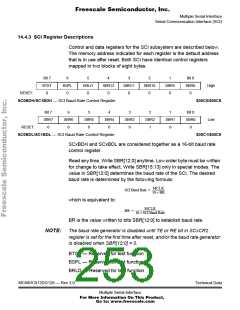
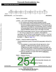
Bit 7
LOOPS
0
6
WOMS
0
5
RSRC
0
4
M
0
3
WAKE
0
2
ILT
0
1
PE
0
Bit 0
PT
0
RESET:
SC0CR1/SC1CR1 — SCI Control Register 1
$00C2/$00CA
Read or write anytime.
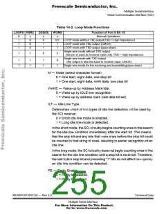
LOOPS — SCI LOOP Mode/Single Wire Mode Enable
0 = SCI transmit and receive sections operate normally.
1 = SCI receive section is disconnected from the RXD pin and the
RXD pin is available as general purpose I/O. The receiver input is
determined by the RSRC bit. The transmitter output is controlled
by the associated DDRS bit. Both the transmitter and the receiver
must be enabled to use the LOOP or the single wire mode.
If the DDRS bit associated with the TXD pin is set during the LOOPS
= 1, the TXD pin outputs the SCI waveform. If the DDRS bit
associated with the TXD pin is clear during the LOOPS = 1, the TXD
pin becomes high (IDLE line state) for RSRC = 0 and high impedance
for RSRC = 1. Refer to Table 14-2.
WOMS — Wired-Or Mode for Serial Pins
This bit controls the two pins (TXD and RXD) associated with the SCIx
section.
0 = Pins operate in a normal mode with both high and low drive
capability. To affect the RXD bit, that bit would have to be
configured as an output (via DDS0/2) which is the single wire
case when using the SCI. WOMS bit still affects general-purpose
output on TXD and RXD pins when SCIx is not using these pins.
1 = Each pin operates in an open drain fashion if that pin is
declared as an output.
RSRC — Receiver Source
When LOOPS = 1, the RSRC bit determines the internal feedback
path for the receiver.
0 = Receiver input is connected to the transmitter internally (not
TXD pin)
1 = Receiver input is connected to the TXD pin
Technical Data
MC68HC912DG128 — Rev 3.0
Multiple Serial Interface
For More Information On This Product,
Go to: www.freescale.com

 FREESCALE [ Freescale ]