Freescale Semiconductor, Inc.
Multiple Serial Interface
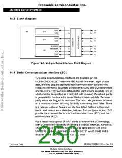
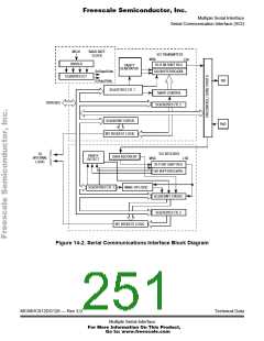
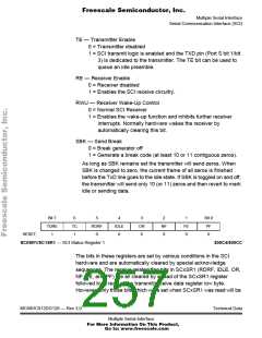
Serial Communication Interface (SCI)
14.4.3 SCI Register Descriptions
Control and data registers for the SCI subsystem are described below.
The memory address indicated for each register is the default address
that is in use after reset. Both SCI have identical control registers
mapped in two blocks of eight bytes.
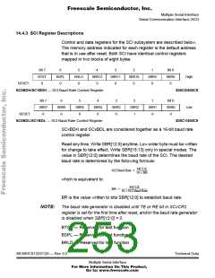
Bit 7
BTST
0
6
BSPL
0
5
BRLD
0
4
SBR12
0
3
SBR11
0
2
SBR10
0
1
SBR9
0
Bit 0
SBR8
0
High
RESET:
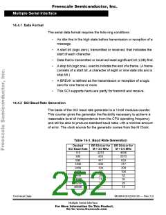
SC0BDH/SC1BDH — SCI Baud Rate Control Register
$00C0/$00C8
Bit 7
SBR7
0
6
SBR6
0
5
SBR5
0
4
SBR4
0
3
SBR3
0
2
SBR2
1
1
SBR1
0
Bit 0
SBR0
0
Low
RESET:
SC0BDL/SC1BDL — SCI Baud Rate Control Register
$00C1/$00C9
SCxBDH and SCxBDL are considered together as a 16-bit baud rate
control register.
Read any time. Write SBR[12:0] anytime. Low order byte must be written
for change to take effect. Write SBR[15:13] only in special modes. The
value in SBR[12:0] determines the baud rate of the SCI. The desired
baud rate is determined by the following formula:
MCLK
SCI Baud Rate = --------------------
16 × BR
which is equivalent to:
MCLK
BR = -----------------------------------------------
16 × SCI Baud Rate
BR is the value written to bits SBR[12:0] to establish baud rate.
NOTE: The baud rate generator is disabled until TE or RE bit in SCxCR2
register is set for the first time after reset, and/or the baud rate generator
is disabled when SBR[12:0] = 0.
BTST — Reserved for test function
BSPL — Reserved for test function
BRLD — Reserved for test function
MC68HC912DG128 — Rev 3.0
Technical Data
Multiple Serial Interface
For More Information On This Product,
Go to: www.freescale.com

 FREESCALE [ Freescale ]