Freescale Semiconductor, Inc.
Multiple Serial Interface
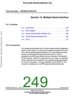
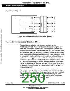
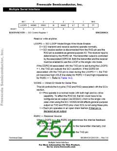
14.3 Block diagram
RxD0
TxD0
PS0
PS1
MSI
SCI0
SCI1
E
RxD1
TxD1
R
PS2
PS3
V
L
D
C
/IO
R
D
MISO/SISO
MOSI/MOMI
SCK
PS4
PS5
PS6
PS7
R
O
SPI
CS/SS
Figure 14-1. Multiple Serial Interface Block Diagram
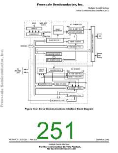
14.4 Serial Communication Interface (SCI)
Two serial communication interfaces are available on the
MC68HC912DG128. These are NRZ format (one start, eight or nine
data, and one stop bit) asynchronous communication systems with
independent internal baud rate generation circuitry and SCI transmitters
and receivers. They can be configured for eight or nine data bits (one of
which may be designated as a parity bit, odd or even). If enabled, parity
is generated in hardware for transmitted and received data. Receiver
parity errors are flagged in hardware. The baud rate generator is based
on a modulus counter, allowing flexibility in choosing baud rates. There
is a receiver wake-up feature, an idle line detect feature, a loop-back
mode, and various error detection features. Two port pins for each SCI
provide the external interface for the transmitted data (TXD) and the
received data (RXD).
For a faster wake-up out of WAIT mode by a received SCI message,
both SCI have the capability of sending a receiver interrupt, if enabled,
when RAF (receiver active flag) is set. For compatibility with other
M68HC12 products, this feature is active only in WAIT mode and is
disabled when VDDPLL supply is at VSS level.
Technical Data
MC68HC912DG128 — Rev 3.0
Multiple Serial Interface
For More Information On This Product,
Go to: www.freescale.com

 FREESCALE [ Freescale ]