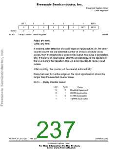
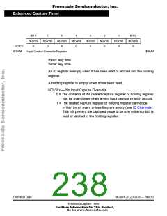
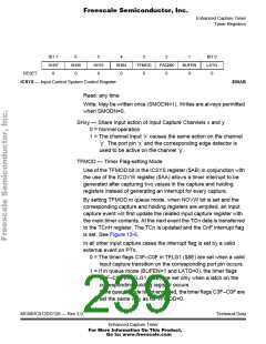
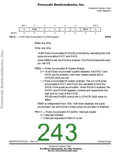
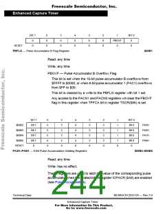
Freescale Semiconductor, Inc.
Enhanced Capture Timer
Timer Registers
BIT 7
6
0
0
5
0
0
4
0
0
3
0
0
2
0
0
1
TCBYP
0
BIT 0
0
0
0
RESET:
0
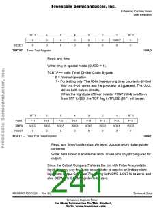
TIMTST — Timer Test Register
$00AD
Read: any time
Write: only in special mode (SMOD = 1).
TCBYP — Main Timer Divider Chain Bypass
0 = Normal operation
1 = For testing only. The 16-bit free-running timer counter is divided
into two 8-bit halves and the prescaler is bypassed. The clock
drives both halves directly.
When the high byte of timer counter TCNT ($84) overflows
from $FF to $00, the TOF flag in TFLG2 ($8F) will be set.
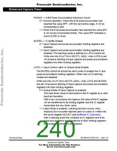
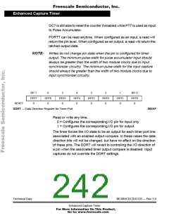
BIT 7
PT7
I/OC7
0
6
PT6
I/OC6
0
5
PT5
I/OC5
0
4
PT4
I/OC4
0
3
PT3
I/OC3
0
2
PT2
I/OC2
0
1
PT1
I/OC1
0
BIT 0
PT0
I/OC0
0
PORT
TIMER
RESET:
PORTT — Timer Port Data Register
$00AE
Read: any time (inputs return pin level; outputs return data register
contents)
Write: data stored in an internal latch (drives pins only if configured for
output)
Since the Output Compare 7 shares the pin with Pulse Accumulator
input, the only way for Pulse accumulator to receive an independent
input from Output Compare 7 is setting both OM7 & OL7 to be zero, and
also OC7M7 in OC7M register to be zero.
MC68HC912DG128 — Rev 3.0
Technical Data
Enhanced Capture Timer
For More Information On This Product,
Go to: www.freescale.com

 FREESCALE [ Freescale ]