Freescale Semiconductor, Inc.
Flash Memory
Operation
7.8 Operation
The Flash EEPROM can contain program and data. On reset, it can
operate as a bootstrap memory to provide the CPU with internal
initialization information during the reset sequence.
7.8.1 Bootstrap Operation Single-Chip Mode
After reset, the CPU controlling the system will begin booting up by
fetching the first program address from address $FFFE.
7.8.2 Normal Operation
The Flash EEPROM allows a byte or aligned word read/write in one bus
cycle. Misaligned word read/write require an additional bus cycle. The
Flash EEPROM array responds to read operations only. Write
operations are ignored.
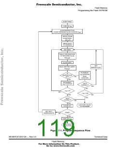
7.8.3 Program/Erase Operation
An unprogrammed Flash EEPROM bit has a logic state of one. A bit
must be programmed to change its state from one to zero. Erasing a bit
returns it to a logic one. The Flash EEPROM has a minimum
program/erase life of 100 cycles. Programming or erasing the Flash
EEPROM is accomplished by a series of control register writes and a
write to a set of programming latches.
Programming is restricted to a single byte or aligned word at a time as
determined by internal signal SZ8 and ADDR[0]. The Flash EEPROM
must first be completely erased prior to programming final data values.
It is possible to program a location in the Flash EEPROM without erasing
the entire array if the new value does not require the changing of bit
values from zero to one.
Read/Write Accesses During Program/Erase — During program or
erase operations, read and write accesses may be different from those
during normal operation and are affected by the state of the control bits
in the Flash EEPROM control register (FEECTL). The next write to any
MC68HC912DG128 — Rev 3.0
Technical Data
Flash Memory
For More Information On This Product,
Go to: www.freescale.com

 FREESCALE [ Freescale ]