F81438
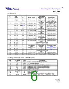
4.2.Transceiver
Description
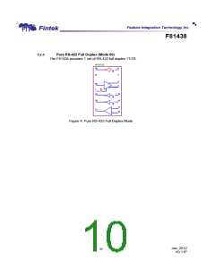
Full-Duplex
T Driver
Enable Active
High
T(B) Driver
Output
T(A) Driver
Output
Pin
Name
Pin
Type
Single Ended
Half-Duplex
T Driver Enable
Active High, R
1
T1_IN
INt
T1 Driver input
Enable Active Low
R(B) Receiver Intput,
T (B) Output
T(A) Driver Output,
R(A) Receiver Input
3
4
R5_IN
R4_IN
AIN/AOUT R5 Receiver Input
AIN/AOUT R4 Receiver Input
High
Impedance
High
Impedance
High
Impedance
High
Impedance
R(A) Receiver
Input
R(B) Receiver
Input
6
R1_IN
AIN
AOUT
AIN
R1 Receiver Input
T1 Driver Output
R2 Receiver Input
R3 Receiver Input
T2 Driver Output
T3 Driver Output
High Impedance
High Impedance
High Impedance
High Impedance
High Impedance
High Impedance
7
T1_OUT
R2_IN
15
16
17
18
R3_IN
AIN
T2_OUT
T3_OUT
AIN
AIN
19
20
R2_OUT
R3_OUT
O4
O4
R2 Reveiver Output High
R3 Receiver Output High
R4 Receiver
Output
R5 Receiver
Output
R Receiver
Output
High
Impedance
R Receiver Output
21
R4_OUT
O4
High
R Receiver Output
High
22
26
27
28
R5_OUT
R1_OUT
T3_IN
O4
O4
INt
INt
R1 Receiver Output High
High
Impedance
T Driver Input
T3 Driver Input
T2 Driver Input
High Impedance
T Driver Input
T2_IN
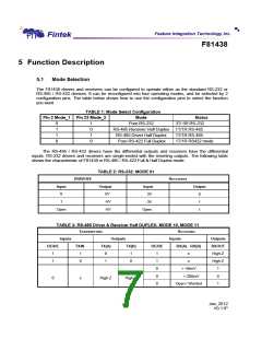
4.3.Charge Pump, Mode Select & Other Functions
Pin
Pin Name
Type
Description
9
C1+
Pump
Positive terminal of the flying capacitor
10
V+
Pump
VDD storage capacitor
11
12
13
14
2
C2+
C1-
C2-
Pump
Pump
Pump
Pump
INt
Positive terminal of negative flying capacitor
Negative terminal of positive flying capacitor
Negative terminal of positive flying capacitor
VSS Storage capacitor
Mode selection pin-1
Mode selection pin-2
V-
MODE_1
MODE_2
SD
INt
23
24
INt
Shutdown pin.
Slew rate control pin, Logical Low input will limit driver
slew from either RS-232 to 1Mbps or RS-485 to 10Mbps
INt,pu 8uA
25
SLEW
Jan, 2012
V0.11P
6

 FINTEK [ FEATURE INTEGRATION TECHNOLOGY INC. ]