F81438
6 Electrical Characteristics Request
6.1
Absolute Maximum Ratings
PARAMETER
RATING
+6.0
UNIT
V
V
Power Supply Voltage
-13.2 to +13.2
-0.3 to Vcc +0.5
-7.5 to +12.5
Continous
-65 to +150
+300
Receiver Input Voltage (DC input Voltage)
Input Voltage at TTL input Pins
Driver Output Voltage (from Ground)
Short Cirecuit Duration, TXOUT to GND
Storage Tempreature
V
V
-
° C
° C
Lead Temperature (soldering, 10s)
Note: Exposure to conditions beyond those listed under Absolute Maximum Ratings may adversely affect the life and
reliability of the device
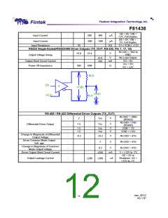
6.2
DC Characteristics
(TA = 0° C to 70° C, VDD = +5.0V ± 5% )
Parameter
Conditions
No Load, MODE = 01.
No Load, MODE = 10, 11.
MODE = 00.
MIN
TYP MAX Unit
Supply Current (RS-232)
Supply Current (RS-485)
Supply Current (RS-422)
2
2
2
30
mA
mA
mA
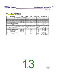
(TA = 0° C to 70° C, VDD = +5.0V ± 5%)
PARAMETER
SYM.
MIN.
TYP.
MAX. UNIT
CONDITIONS
Transmitter and Logic Input Pins (MODE, SLEW) 1, 2, 23, 24, 25, 27, 28
Logic Input Voltage HIGH
Logic Input Voltage LOW
Logic Input Pull-up Current
TX_IN Pull High Current
Logic Input Hysteresis
VIL
-
2.4
V
V
VDD = 5.0 V
0.8
±15
±15
-
μA
μA
V
IIT
-
0.5
RS-232 and RS-485 / 422 Receiver Outputs RX_OUT: Pin 19, 20, 21, 22, 26
Vcc-
0.6
Receiver Output Voltage HIGH
VOH
VOL
IOS
-
V
V
IOUT = -1.5mA.
IOUT = 2.5mA.
Receiver Output Voltage LOW
Receiver Output Short-Circuit
Current
0.4
±60
±1
mA
0 < Vo < Vcc.
±20
Receiver Output Leakage Current
μA
Receivers Disabled.
±0.05
RS-232 Single-End Receiver Input (RX_IN, pin 3, 4, 6, 15, 16)
Input Voltage Range
Input Threshold Low
Input Threshold HIGH
Input Hysteresis
-
VIL
VIH
-
-13.2
0.8
+13.2
2.4
7
V
V
V
V
KΩ
1.5
1.8
0.5
5
VCC = 5.0V.
VCC = 5.0V.
Input Resistance
-
3
RS-485 / RS-422 Differential Receiver Inputs (RX_IN, pin 3, 4)
Receiver Differential Threshold
Voltage
-
-
-250
-200
30
mV
mV
VB = 0V.
Receiver Input Hysteresis
VCM = 0V.
Jan, 2012
V0.11P
11

 FINTEK [ FEATURE INTEGRATION TECHNOLOGY INC. ]