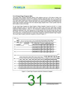
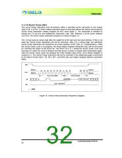
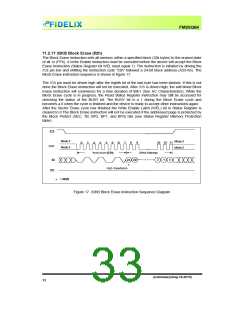
FM25Q64ꢀ
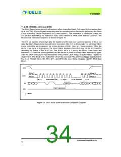
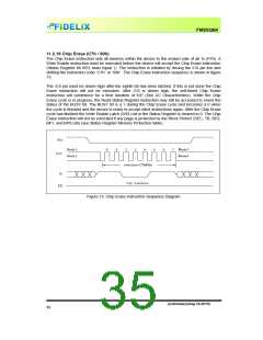
11.2.19ꢀChipꢀEraseꢀ(C7hꢀ/ꢀ60h)ꢀ
TheꢀChipꢀEraseꢀinstructionꢀsetsꢀallꢀmemoryꢀwithinꢀtheꢀdeviceꢀtoꢀtheꢀerasedꢀsateꢀofꢀallꢀ1sꢀ(FFh).ꢀAꢀ
WriteꢀEnableꢀinstructionꢀmustꢀbeꢀexecutedꢀbeforeꢀtheꢀdeviceꢀwillꢀacceptꢀtheꢀChipꢀEraseꢀInstructionꢀ
(StatusꢀRegisterꢀbitꢀWELꢀmustꢀequalꢀ1).ꢀTheꢀinstructionꢀisꢀinitiatedꢀbyꢀdrivingꢀtheꢀ/CSꢀpinꢀlowꢀandꢀ
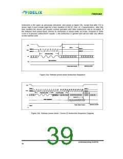
shiftingꢀtheꢀinstructionꢀcodeꢀ“C7h”ꢀorꢀ“60h”.ꢀTheꢀChipꢀEraseꢀinstructionꢀsequenceꢀisꢀshownꢀinꢀfigureꢀ
19.ꢀ
ꢀ
Theꢀ/CSꢀpinꢀmustꢀbeꢀdrivenꢀhighꢀafterꢀtheꢀeighthꢀbitꢀhasꢀbeenꢀlatched.ꢀIfꢀthisꢀisꢀnotꢀdoneꢀtheꢀChipꢀ
Eraseꢀ instructionꢀ willꢀ notꢀ beꢀ executed.ꢀ Afterꢀ /CSꢀ isꢀ drivenꢀ high,ꢀ theꢀ selfꢁtimedꢀ Chipꢀ Eraseꢀ
instructionꢀ willꢀ commenceꢀ forꢀ aꢀ timeꢀ durationꢀ ofꢀ tCEꢀ (Seeꢀ ACꢀ Characteristics).ꢀ Whileꢀ theꢀ Chipꢀ
Eraseꢀcycleꢀisꢀinꢀprogress,ꢀtheꢀReadꢀStatusꢀRegisterꢀinstructionꢀmayꢀstillꢀbeꢀaccessedꢀtoꢀcheckꢀtheꢀ
statusꢀofꢀtheꢀBUSYꢀbit.ꢀTheꢀBUSYꢀbitꢀisꢀaꢀ1ꢀduringꢀtheꢀChipꢀEraseꢀcycleꢀandꢀbecomesꢀaꢀ0ꢀwhenꢀ
theꢀcycleꢀisꢀfinishedꢀandꢀtheꢀdeviceꢀisꢀreadyꢀtoꢀacceptꢀotherꢀinstructionsꢀagain.ꢀAfterꢀtheꢀChipꢀEraseꢀ
cycleꢀhasꢀfinishedꢀtheꢀWriteꢀEnableꢀLatchꢀ(WEL)ꢀbitꢀinꢀtheꢀStatusꢀRegisterꢀisꢀclearedꢀtoꢀ0.ꢀTheꢀChipꢀ
EraseꢀinstructionꢀwillꢀnotꢀbeꢀexecutedꢀifꢀanyꢀpageꢀisꢀprotectedꢀbyꢀtheꢀBlockꢀProtectꢀ(SEC,ꢀTB,ꢀBP2,ꢀ
BP1,ꢀandꢀBP0)ꢀbitsꢀ(seeꢀStatusꢀRegisterꢀMemoryꢀProtectionꢀtable).ꢀ
ꢀ
ꢀ
Figureꢀ19.ꢀChipꢀEraseꢀInstructionꢀSequenceꢀDiagramꢀ
ꢀ
ꢀ
ꢀ
ꢀ
ꢀ
ꢀ
ꢀ
ꢀ
ꢀ
ꢀ
ꢀ
ꢀ
ꢀ
ꢀ
ꢀ
ꢀ
ꢀ
ꢀ
ꢀ
ꢀ
ꢀ
preliminary(Aug.18.2010)ꢀ ꢀ ꢀ ꢀ
35ꢀ

 FIDELIX [ FIDELIX ]