FM25Q64ꢀ
ꢀ
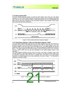
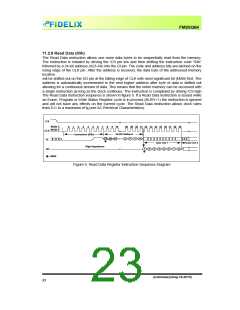
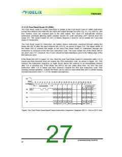
11.2.9ꢀReadꢀDataꢀ(03h)ꢀ
TheꢀReadꢀDataꢀinstructionꢀallowsꢀoneꢀmoreꢀdataꢀbytesꢀtoꢀbeꢀsequentiallyꢀreadꢀfromꢀtheꢀmemory.ꢀ
Theꢀinstructionꢀisꢀinitiatedꢀbyꢀdrivingꢀtheꢀ/CSꢀpinꢀlowꢀandꢀthenꢀshiftingꢀtheꢀinstructionꢀcodeꢀ“03h”ꢀ
followedꢀbyꢀaꢀ24ꢁbitꢀaddressꢀ(A23ꢁA0)ꢀintoꢀtheꢀDIꢀpin.ꢀTheꢀcodeꢀandꢀaddressꢀbitsꢀareꢀlatchedꢀonꢀtheꢀ
risingꢀedgeꢀofꢀtheꢀCLKꢀpin.ꢀAfterꢀtheꢀaddressꢀisꢀreceived,ꢀtheꢀdataꢀbyteꢀofꢀtheꢀaddressedꢀmemoryꢀ
locationꢀ
willꢀbeꢀshiftedꢀoutꢀonꢀtheꢀDOꢀpinꢀatꢀtheꢀfallingꢀedgeꢀofꢀCLKꢀwithꢀmostꢀsignificantꢀbitꢀ(MSB)ꢀfirst.ꢀTheꢀ
addressꢀisꢀautomaticallyꢀincrementedꢀtoꢀtheꢀnextꢀhigherꢀaddressꢀafterꢀbyteꢀofꢀdataꢀisꢀshiftedꢀoutꢀ
allowingꢀforꢀaꢀcontinuousꢀstreamꢀofꢀdata.ꢀThisꢀmeansꢀthatꢀtheꢀentireꢀmemoryꢀcanꢀbeꢀaccessedꢀwithꢀ
aꢀsingleꢀinstructionꢀasꢀlongꢀasꢀtheꢀclockꢀcontinues.ꢀTheꢀinstructionꢀisꢀcompletedꢀbyꢀdrivingꢀ/CSꢀhigh.ꢀ
TheꢀReadꢀDataꢀinstructionꢀsequenceꢀisꢀshownꢀinꢀfigureꢀ9.ꢀIfꢀaꢀReadꢀDataꢀinstructionꢀisꢀissuedꢀwhileꢀ
anꢀErase,ꢀProgramꢀorꢀWriteꢀStatusꢀRegisterꢀcycleꢀisꢀinꢀprocessꢀ(BUSY=1)ꢀtheꢀinstructionꢀisꢀignoredꢀ
andꢀwillꢀnotꢀhaveꢀanyꢀeffectsꢀonꢀtheꢀcurrentꢀcycle.ꢀTheꢀReadꢀDataꢀinstructionꢀallowsꢀclockꢀratesꢀ
fromꢀD.CꢀtoꢀaꢀmaximumꢀofꢀfRꢀ(seeꢀACꢀElectricalꢀCharacteristics).ꢀ
ꢀ
/CS
Modeꢀ3
Modeꢀ0
0
1
2
3
4
5
6
7
8
9
10
28 29 30 31 32 33 34 35 36 37 38 39
CLK
DI
24ꢁBitꢀAddress
23 22 21
1
Instructionꢀ(03h)
3
2
0
DataꢀOutꢀ1
DataꢀOutꢀ2
HighꢀImpedance
2
7
6
5
4
3
1
0
7
DO
=MSB
ꢀ
Figureꢀ9.ꢀReadꢀDataꢀRegisterꢀInstructionꢀSequenceꢀDiagramꢀ
ꢀ
ꢀ
ꢀ
ꢀ
ꢀ
ꢀ
ꢀ
ꢀ
ꢀ
ꢀ
ꢀ
ꢀ
ꢀ
ꢀ
ꢀ
ꢀ
ꢀ
ꢀ
ꢀ
ꢀ
ꢀ
ꢀ
ꢀ
ꢀ
preliminary(Aug.18.2010)ꢀ ꢀ ꢀ ꢀ
23ꢀ

 FIDELIX [ FIDELIX ]