FM25Q64ꢀ
ꢀ
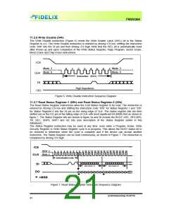
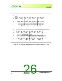
11.2.8ꢀWriteꢀStatusꢀRegisterꢀ(01h)ꢀ
Theꢀ Writeꢀ Statusꢀ Registerꢀ instructionꢀ allowsꢀ theꢀ Statusꢀ Registerꢀ toꢀ beꢀ written.ꢀ Aꢀ Writeꢀ Enableꢀ
instructionꢀmustꢀpreviouslyꢀhaveꢀbeenꢀexecutedꢀforꢀtheꢀdeviceꢀtoꢀacceptꢀtheꢀWriteꢀStatusꢀRegisterꢀ
Instructionꢀ(StatusꢀRegisterꢀbitꢀWELꢀmustꢀequalꢀ1).ꢀOnceꢀwriteꢀisꢀenabled,ꢀtheꢀinstructionꢀisꢀenteredꢀ
byꢀdrivingꢀ/CSꢀlow,ꢀsendingꢀtheꢀinstructionꢀcodeꢀ“01h”,ꢀandꢀthenꢀwritingꢀtheꢀstatusꢀregisterꢀdataꢀbyteꢀ
orꢀ wordꢀ asꢀillustratedꢀ inꢀfigureꢀ 8.ꢀ Theꢀ Statusꢀ Registerꢀbitsꢀ areꢀ shownꢀ inꢀ figureꢀ 3ꢀ andꢀdescribedꢀ
earlierꢀinꢀthisꢀdatasheet.ꢀ
ꢀ
OnlyꢀnonꢁvolatileꢀStatusꢀRegisterꢀbitsꢀSRP0,ꢀSEC,ꢀTB,ꢀBP2,ꢀBP1,ꢀBP0ꢀ(bitsꢀ7,ꢀ5,ꢀ4,ꢀ3,ꢀ2ꢀofꢀStatusꢀ
Registerꢁ1)ꢀandꢀQE,ꢀSRP1ꢀ(bitsꢀ9ꢀandꢀ8ꢀofꢀStatusꢀRegisterꢁ2)ꢀcanꢀbeꢀwrittenꢀto.ꢀAllꢀotherꢀStatusꢀ
RegisterꢀbitꢀlocationsꢀareꢀreadꢁonlyꢀandꢀwillꢀnotꢀbeꢀaffectedꢀbyꢀtheꢀWriteꢀStatusꢀRegisterꢀinstruction.ꢀ
ꢀ
Theꢀ/CSꢀpinꢀmustꢀbeꢀdrivenꢀhighꢀafterꢀtheꢀeighthꢀorꢀsixteenthꢀbitꢀofꢀdataꢀthatꢀisꢀclockedꢀin.ꢀIfꢀthisꢀisꢀ
notꢀdoneꢀtheꢀWriteꢀStatusꢀRegisterꢀinstructionꢀwillꢀnotꢀbeꢀexecuted.ꢀIfꢀ/CSꢀisꢀdrivenꢀhighꢀafterꢀtheꢀ
eighthꢀclock,ꢀtheꢀQEꢀandꢀSRP1ꢀbitsꢀwillꢀbeꢀcleared to 0.ꢀAfterꢀ/CSꢀisꢀdrivenꢀhigh,ꢀtheꢀselfꢁtimedꢀ
WriteꢀStatusꢀRegisterꢀcycleꢀwillꢀcommenceꢀforꢀaꢀtimeꢀdurationꢀofꢀtwꢀ(SeeꢀACꢀCharacteristics).ꢀWhileꢀ
theꢀWriteꢀStatusꢀRegisterꢀcycleꢀisꢀinꢀprogress,ꢀtheꢀReadꢀStatusꢀRegisterꢀinstructionꢀmayꢀstillꢀbeꢀ
accessedꢀtoꢀcheckꢀtheꢀstatusꢀofꢀtheꢀBUSYꢀbit.ꢀTheꢀBUSYꢀbitꢀisꢀaꢀ1ꢀduringꢀtheꢀWriteꢀStatusꢀRegisterꢀ
cycleꢀandꢀaꢀ0ꢀwhenꢀtheꢀcycleꢀisꢀfinishedꢀandꢀreadyꢀ toꢀacceptꢀotherꢀinstructionsꢀagain.ꢀAfterꢀtheꢀ
WriteꢀStatusꢀRegisterꢀcycleꢀhasꢀfinished,ꢀTheꢀWriteꢀEnableꢀLatchꢀ(WEL)ꢀbitꢀinꢀStatusꢀRegisterꢀwillꢀ
beꢀclearedꢀtoꢀ0.ꢀ
ꢀ
TheꢀWriteꢀStatusꢀRegisterꢀinstructionꢀallowsꢀtheꢀBlockꢀProtectꢀbitsꢀ(SEC,ꢀTB,ꢀBP2,ꢀBP1ꢀandꢀBP0)ꢀ
toꢀbeꢀsetꢀforꢀprotectingꢀall,ꢀaꢀportion,ꢀorꢀnoneꢀofꢀtheꢀmemoryꢀfromꢀeraseꢀandꢀprogramꢀinstructions.ꢀ
Protectedꢀareasꢀbecomeꢀreadꢁonlyꢀ(seeꢀStatusꢀRegisterꢀMemoryꢀProtectionꢀtableꢀandꢀdescription).ꢀ
TheꢀWriteꢀStatusꢀRegisterꢀinstructionꢀalsoꢀallowsꢀtheꢀStatusꢀRegisterꢀProtectꢀbitsꢀ(SRP0,ꢀSRP1)ꢀtoꢀ
beꢀ set.ꢀ Thoseꢀ bitsꢀ areꢀ usedꢀ inꢀ conjunctionꢀ withꢀ theꢀ Writeꢀ protectꢀ (/WP)ꢀ pin,ꢀ Lockꢀ outꢀ orꢀ OTPꢀ
featuresꢀtoꢀdisableꢀwritesꢀtoꢀtheꢀstatusꢀregister.ꢀ Pleaseꢀreferꢀtoꢀ11.1.16ꢀforꢀdetailedꢀdescriptionsꢀ
StatusꢀRegisterꢀprotectionꢀmethods.ꢀFactoryꢀdefaultꢀallꢀStatusꢀRegisterꢀbitsꢀareꢀ0.ꢀ
ꢀ
ꢀ
/CS
Modeꢀ3
Modeꢀ0
Modeꢀ3
Modeꢀ0
0
1
2
3
4
5
6
7
8
9
10 11 12 13 14 15 16 17 18 19 20 21 22 23
CLK
StatusꢀRegister1ꢀIn
Instructionꢀ(01h)
StatusꢀRegister2ꢀIn
2
6
5
4
3
X
X
X
9
7
X
X
X
X
X
8
DI
HighꢀImpedance
DO
=MSB
ꢀ
ꢀ
Figureꢀ8.ꢀWriteꢀStatusꢀRegisterꢀInstructionꢀSequenceꢀDiagramꢀ
ꢀ
ꢀ
ꢀ
ꢀ
ꢀ
ꢀ
ꢀ
preliminary(Aug.18.2010)ꢀ ꢀ ꢀ ꢀ
22ꢀ

 FIDELIX [ FIDELIX ]