Product Specification
Highly Integrated Green-Mode PWM Controller
SG5841/J
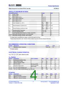
ABSOLUTE MAXIMUM RATINGS
Symbol Parameter
Value
30
Unit
V
VVDD
VVIN
VFB
Supply Voltage
Input Terminal
30
V
Input Voltage to FB Pin
Input Voltage to SENSE Pin
Input Voltage to RT Pin
Input Voltage to RI Pin
-0.3 to 7.0
-0.3 to 7.0
-0.3 to 7.0
-0.3 to 7.0
DIP
V
VSENSE
VRT
V
V
VRI
V
800.0
400.0
82.5
PD
Power Dissipation (TA < 50°C )
mW
SOP
DIP
R
Thermal Resistance (Junction-to-Air)
Thermal Resistance (Junction-to-Case)
°C/W
°C/W
ΘJA
SOP
141.0
59.7
DIP
ΘJC
R
SOP
80.8
TJ
Operating Junction Temperature
-40 to +125
-55 to +150
260
°C
°C
°C
KV
V
TSTG
TL
Storage Temperature Range
Lead Temperature (Wave Soldering or Infrared, 10 Seconds)
VESD,HBM Electrostatic Discharge Capability, Human Body Model
VESD,MM Electrostatic Discharge Capability, Machine Model
3.0
250
* All voltage values, except differential voltages, are given with respect to GND pin.
* Stresses beyond those listed under "absolute maximum ratings" may cause permanent damage to the device.
RECOMMENDED OPERATING CONDITIONS
Symbol
Parameter
Value
Unit
TA
Operating Ambient Temperature
-20 to +85
°C
* For proper operation.
ELECTRICAL CHARACTERISTICS
VDD = 15V, TA = 25°C, unless otherwise noted.
VDD Section
Symbol
VDD-OP
Parameter
Test Condition
Min.
Typ.
Max.
24.7
17
Unit
V
Continuously Operating Voltage
Start Threshold Voltage
Minimum Operating Voltage
Start-up Current
VDD-ON
VDD-OFF
IDD-ST
15
9
16
10
14
V
11
V
VDD=VDD-ON–0.16V
VDD=15V, RI=26KΩ,
GATE=OPEN
30
µA
IDD-OP
Operating Supply Current
4
5
mA
VDD-CLAMP
VDD Over-Voltage-Clamping Level
28
50
29
V
tD-VDDCLAMP
VDD Over-Voltage-Clamping Debounce Time RI=26KΩ
100
200
µs
RI Section
Symbol
RINOR
Parameter
RI Operating Range
Test Condition
Min.
15.5
Typ.
Max.
36.0
Unit
KΩ
RIMAX
Maximum RI Value for Protection
Minimum RI Value for Protection
230
10
KΩ
RIMIN
KΩ
© System General Corp.
Version 1.3.1 (IAO33.0017.B6)
- 4 -
www.sg.com.tw • www.fairchildsemi.com
September 20, 2007

 FAIRCHILD [ FAIRCHILD SEMICONDUCTOR ]