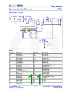
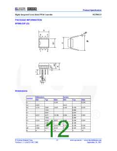
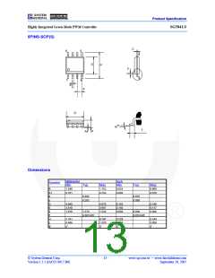
Product Specification
Highly Integrated Green-Mode PWM Controller
SG5841/J
When VDD goes below the turn-off threshold (e.g., 10V)
the controller is totally shut down. VDD is charged up to
the turn-on threshold voltage of 16V through the start-up
resistor until PWM output is restarted. This protection
feature remains activated as long as the over-loading
condition persists. This prevents the power supply from
overheating due to over loading conditions.
Constant Output Power Limit
When the SENSE voltage across the sense resistor, RS,
reaches the threshold voltage, around 0.85V, the output
GATE drive is turned off after delay tPD. This delay
introduces additional current, proportional to tPD • VIN / LP.
The delay is nearly constant regardless of the input voltage
VIN. Higher input voltage results in larger additional
current and the output power limit is higher than under low
input line voltage. To compensate this variation for a wide
AC input range, a sawtooth power-limiter (saw limiter) is
designed to solve the unequal power-limit problem. The
Noise Immunity
Noise on the current sense or control signal may cause
significant pulse width jitter, particularly in the
continuous-conduction mode. Slope compensation helps
alleviate this problem. Good placement and layout
practices should be followed. Avoiding long PCB traces
and component leads, locating compensation and filter
components near to the SG5841/J, and increasing the
power MOS gate resistance improves performance.
saw limiter is designed as a positive ramp signal (Vlimit_ramp
)
and fed to the inverting input of the OCP comparator. This
results in a lower current limit at high-line inputs than at
low-line inputs.
VDD Over-Voltage Clamping
VDD over-voltage clamping has been built in to prevent
damage due to abnormal conditions. Once the VDD
voltage is over the VDD over-voltage clamping voltage
(VDD-CLAMP) and lasts for tD-VDDCLAMP, the PWM pulses are
disabled until the VDD voltage drops below the VDD
over-voltage clamping voltage.
Thermal Protection
An NTC thermistor RNTC in series with a resistor RA can
be connected from pin RT to ground. A constant current
IRT is output from pin RT. The voltage on the RT pin can
be expressed as VRT = IRT × (RNTC + RA), in which IRT = 2
x (1.3V / RI). At high ambient temperature, RNTC is
smaller, such that VRT decreases. When VRT is less than
0.62V, the PWM is completely turned off.
Limited Power Control
The FB voltage increases every time the output of the
power supply is shorted or over loaded. If the FB voltage
remains higher than a built-in threshold longer than tD-OLP
,
PWM output is turned off. As PWM output is turned off,
the supply voltage VDD begins decreasing.
----------------- (2)
tD - OLP (ms) = 1.115 ×R (KΩ)
I
© System General Corp.
Version 1.3.1 (IAO33.0017.B6)
- 10 -
www.sg.com.tw • www.fairchildsemi.com
September 20, 2007

 FAIRCHILD [ FAIRCHILD SEMICONDUCTOR ]