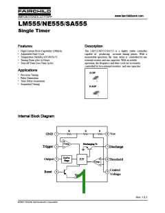
LM555/NE555/SA555
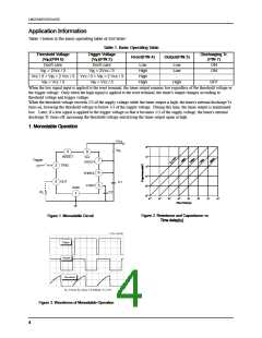
Figure 1 illustrates a monostable circuit. In this mode, the timer generates a fixed pulse whenever the trigger voltage falls
below Vcc/3. When the trigger pulse voltage applied to the #2 pin falls below Vcc/3 while the timer output is low, the timer's
internal flip-flop turns the discharging Tr. off and causes the timer output to become high by charging the external capacitor C1
and setting the flip-flop output at the same time.
The voltage across the external capacitor C1, V increases exponentially with the time constant t=R *C and reaches 2Vcc/3
C1
A
at td=1.1R *C. Hence, capacitor C1 is charged through resistor R . The greater the time constant R C, the longer it takes
A
A
A
for the V to reach 2Vcc/3. In other words, the time constant R C controls the output pulse width.
C1
A
When the applied voltage to the capacitor C1 reaches 2Vcc/3, the comparator on the trigger terminal resets the flip-flop,
turning the discharging Tr. on. At this time, C1 begins to discharge and the timer output converts to low.
In this way, the timer operating in the monostable repeats the above process. Figure 2 shows the time constant relationship
based on R and C. Figure 3 shows the general waveforms during the monostable operation.
A
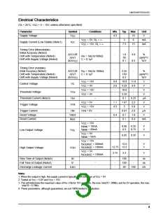
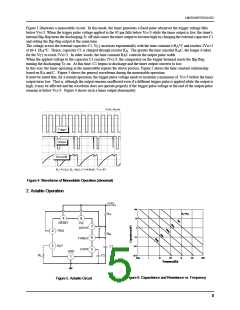
It must be noted that, for a normal operation, the trigger pulse voltage needs to maintain a minimum of Vcc/3 before the timer
output turns low. That is, although the output remains unaffected even if a different trigger pulse is applied while the output is
high, it may be affected and the waveform does not operate properly if the trigger pulse voltage at the end of the output pulse
remains at below Vcc/3. Figure 4 shows such a timer output abnormality.
Figure 4. Waveforms of Monostable Operation (abnormal)
2. Astable Operation
+Vcc
100
(RA+2RB)
R
A
10
1
4
8
RESET
Vcc
7
6
DISCH
TRIG
OUT
2
3
R
B
0.1
THRES
CONT
0.01
C1
5
GND
1E-3
100m
R
C2
L
1
1
10
100
1k
10k
100k
Frequency(Hz)
Figure 6. Capacitance and Resistance vs. Frequency
Figure 5. Astable Circuit
5

 FAIRCHILD [ FAIRCHILD SEMICONDUCTOR ]