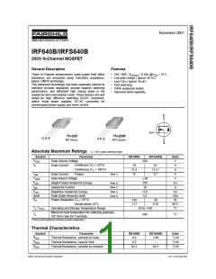
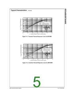
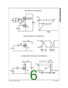
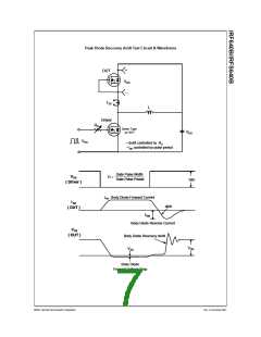
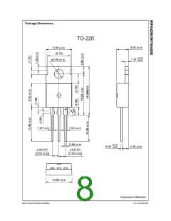
Typical Characteristics
VGS
Top :
15.0V
10.0 V
8.0 V
7.0 V
6.5 V
6.0 V
5.5 V
101
1
10
Bottom: 5.0V
150oC
25oC
0
10
100
-55oC
※
※
Notes :
Notes :
μ
1. V = 40V
2. 250 s Pulse Test
1. 250 s Pulse Test
DS μ
℃
2. TC = 25
-1
10
-1
10
-1
100
101
2
4
6
8
10
10
VGS, Gate-Source Voltage [V]
VDS, Drain-Source Voltage [V]
Figure 1. On-Region Characteristics
Figure 2. Transfer Characteristics
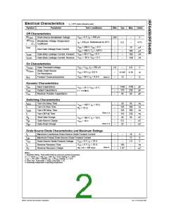
1.0
0.8
0.6
0.4
0.2
0.0
VGS = 10V
VGS = 20V
101
100
℃
150
℃
25
※
Notes :
1. V = 0V
2. 250 s Pulse Test
GS μ
※
℃
Note : T = 25
J
-1
10
0
10
20
30
40
50
60
0.2
0.4
0.6
0.8
1.0
1.2
1.4
1.6
1.8
2.0
ID, Drain Current [A]
VSD, Source-Drain voltage [V]
Figure 3. On-Resistance Variation vs
Drain Current and Gate Voltage
Figure 4. Body Diode Forward Voltage
Variation with Source Current
and Temperature
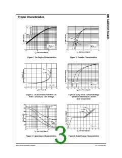
3500
3000
2500
2000
1500
1000
500
12
10
8
C
C
C
iss = Cgs + Cgd (Cds = shorted)
oss = Cds + Cgd
rss = Cgd
VDS = 40V
VDS = 100V
VDS = 160V
C
iss
6
C
oss
4
C
rss
※
Notes :
1. VGS = 0 V
2. f = 1 MHz
2
※
Note: ID = 18 A
0
0
10
-1
0
10
0
5
10
15
20
25
30
35
40
45
50
101
QG, Total Gate Charge [nC]
VDS, Drain-Source Voltage [V]
Figure 5. Capacitance Characteristics
Figure 6. Gate Charge Characteristics
©2001 Fairchild Semiconductor Corporation
Rev. A, November 2001

 FAIRCHILD [ FAIRCHILD SEMICONDUCTOR ]