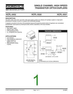
SINGLE CHANNEL HIGH SPEED
TRANSISTOR OPTOCOUPLERS
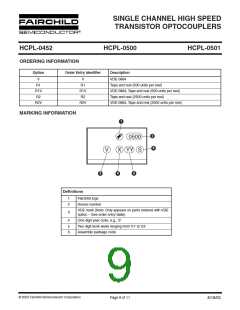
HCPL-0452
HCPL-0500
HCPL-0501
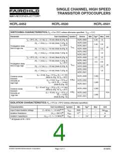
NOTES
1. Derate linearly above 70°C free-air temperature at a rate of 0.8 mA/°C.
2. Derate linearly above 70°C free-air temperature at a rate of 1.6 mA/°C.
3. Derate linearly above 70°C free-air temperature at a rate of 0.9 mW/°C.
4. Derate linearly above 70°C free-air temperature at a rate of 2.0 mW/°C.
5. Current Transfer Ratio is defined as a ratio of output collector current, I , to the forward LED input current, I , times 100%.
O
F
6. The 4.1 kΩ load represents 1 LSTTL unit load of 0.36 mA and 6.1kΩ pull-up resistor.
7. The 1.9 kΩ load represents 1 TTL unit load of 1.6 mA and 5.6 kΩ pull-up resistor.
8. Common mode transient immunity in logic high level is the maximum tolerable (positive) dV /dt on the leading edge of the
cm
common mode pulse signal V , to assure that the output will remain in a logic high state (i.e., V >2.0 V). Common mode tran-
CM
O
sient immunity in logic low level is the maximum tolerable (negative) dV /dt on the trailing edge of the common mode pulse
cm
signal, VCM, to assure that the output will remain in a logic low state (i.e., V <0.8 V).
O
9. Device is considered a two terminal device: Pins 1, 2, 3 and 4 are shorted together and Pins 5, 6, 7 and 8 are shorted together.
10. 2500 VAC RMS for 1 minute duration is equivalent to 3000 VAC RMS for 1 second duration.
© 2003 Fairchild Semiconductor Corporation
Page 5 of 11
8/18/03

 FAIRCHILD [ FAIRCHILD SEMICONDUCTOR ]