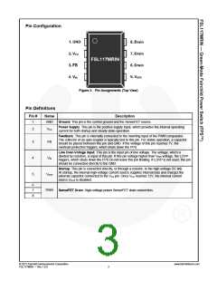
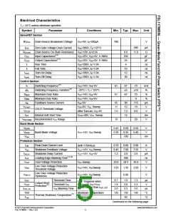
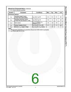
Pin Configuration
Figure 3. Pin Assignments (Top View)
Pin Definitions
Pin #
Name
Description
1
GND
Ground. This pin is the control ground and the SenseFET source.
Power Supply. This pin is the positive supply input, which provides the internal operating
current for both startup and steady-state operation.
2
3
VCC
FB
Feedback. This pin is internally connected to the inverting input of the PWM comparator.
The collector of an opto-coupler is typically tied to this pin. For stable operation, a capacitor
should be placed between this pin and GND. If the voltage of this pin reaches 7V, the
overload protection triggers, which shuts down the FPS.
Line Over-Voltage Input. This pin is the input pin of line voltage. The voltage, which is
divided by resistors, is input of this pin. If this pin voltage higher than VINH voltage, the LOVP
triggers, which shuts down the FPS Do not leave this pin floating. If LOVP is not used, this pin
should be connected directly to the GND.
4
5
VIN
Startup. This pin is connected directly, or through a resistor, to the high-voltage DC link.
At startup, the internal high-voltage current source supplies internal bias and charges the
external capacitor connected to the VCC pin. Once VCC reaches 12V, the internal current
source (ICH) is disabled.
VSTR
6
7
8
Drain
SenseFET Drain. High-voltage power SenseFET drain connection.
© 2012 Fairchild Semiconductor Corporation
FSL117MRN • Rev.1.0.0
www.fairchildsemi.com
3

 FAIRCHILD [ FAIRCHILD SEMICONDUCTOR ]