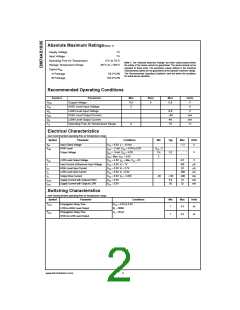
Absolute Maximum Ratings(Note 1)
Supply Voltage
Input Voltage
7V
7V
Operating Free Air Temperature
Storage Temperature Range
Typical θJA
0°C to 70°C
Note 1: The “Absolute Maximum Ratings” are those values beyond which
the safety of the device cannot be guaranteed. The device should not be
operated at these limits. The parametric values defined in the Electrical
Characteristics tables are not guaranteed at the absolute maximum ratings.
The “Recommended Operating Conditions” table will define the conditions
for actual device operation.
−65°C to +150°C
N Package
58.3°C/W
M Package
154.0°C/W
Recommended Operating Conditions
Symbol
Parameter
Min
4.5
2
Nom
Max
Units
V
VCC
VIH
VIL
IOH
IOL
TA
Supply Voltage
5
5.5
HIGH Level Input Voltage
V
LOW Level Input Voltage
0.8
−48
48
V
HIGH Level Output Current
LOW Level Output Current
Operating Free Air Temperature Range
mA
mA
°C
0
70
Electrical Characteristics
over recommended operating free air temperature range
Symbol
Parameter
Input Clamp Voltage
Conditions
Min
Typ
Max
Units
V
V
V
= 4.5V, I = −18 mA
−1.2
V
IK
CC
I
HIGH Level
I
I
I
= −2 mA, V = 4.5V to 5.5V
V
−2
OH
OH
CC
CC
Output Voltage
= −3 mA, V = 4.5V
2.4
3.2
V
OH
OH
CC
= Max, V = 4.5V
2
CC
V
LOW Level Output Voltage
V
V
V
V
V
= 4.5V, I = Max, V = 2V
0.5
100
20
V
OL
CC
CC
CC
CC
CC
OL
IH
I
Input Current at Maximum Input Voltage
HIGH Level Input Current
= 5.5V, V = 7V
µA
µA
µA
mA
mA
mA
I
I
I
= 5.5V, V = 2.7V
I
IH
I
LOW Level Input Current
= 5.5V, V = 0.4V
−500
−200
10
IL
I
I
Output Drive Current
= 5.5V, V = 2.25V
−50
−135
6.5
O
O
I
Supply Current with Outputs HIGH
Supply Current with Outputs LOW
V
= 5.5V
= 5.5V
CC
CCH
CC
I
V
20
32
CCL
Switching Characteristics
over recommended operating free air temperature range
Symbol
Parameter
Propagation Delay Time
Conditions
Min
Max
Units
T
T
V
= 4.5V to 5.5V
= 500Ω
PLH
CC
1
4.3
ns
LOW-to-HIGH Level Output
Propagation Delay Time
HIGH-to-LOW Level Output
R
C
L
= 50 pF
PHL
L
1
4.3
ns
www.fairchildsemi.com
2

 FAIRCHILD [ FAIRCHILD SEMICONDUCTOR ]