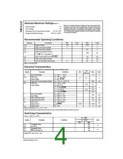
Truth Table
Decimal
or
Inputs
Outputs
Note
Function
LT
H
RBI
H
A3
L
A2
L
A1
L
A0 BI/RBO
a
L
H
L
L
b
L
L
L
L
c
L
L
H
L
d
L
e
L
f
g
H
H
L
0
1
2
3
L
H
L
H
H
H
H
L
(Note 2)
(Note 2)
H
X
L
L
L
H
L
H
L
H
H
H
H
X
L
L
H
H
H
X
L
L
H
L
H
L
4
5
6
7
8
H
H
H
H
H
X
X
X
X
X
L
L
L
L
H
H
H
H
H
L
L
L
L
H
L
H
H
H
H
H
H
L
L
H
H
L
L
L
L
L
L
H
L
H
H
L
L
L
L
H
L
L
L
L
H
L
H
H
L
H
L
L
H
L
H
L
H
L
L
L
9
H
H
H
H
H
X
X
X
X
X
H
H
H
H
H
L
L
L
H
H
L
H
L
H
H
H
H
H
L
H
H
H
L
L
H
H
L
L
H
L
H
L
H
L
L
H
H
L
L
L
L
L
L
10
11
12
13
L
H
L
L
H
H
H
H
H
H
H
H
L
L
H
H
L
14
15
H
H
X
H
L
X
X
X
L
H
H
X
L
H
H
X
L
H
H
X
L
L
H
X
L
H
H
L
H
H
H
H
L
H
H
H
H
L
H
H
H
H
L
L
H
H
H
L
L
H
H
H
L
L
H
H
H
L
L
H
H
H
L
BI
(Note 3)
(Note 4)
(Note 5)
RBI
LT
L
X
X
X
X
X
H
Note 2: BI/RBO is wire-AND logic serving as blanking input (BI) and/or ripple-blanking output (RBO). The blanking out (BI) must be open or held at a HIGH
level when output functions 0 through 15 are desired, and ripple-blanking input (RBI) must be open or at a HIGH level if blanking or a decimal 0 is not
desired. X = input may be HIGH or LOW.
Note 3: When a LOW level is applied to the blanking input (forced condition) all segment outputs go to a HIGH level regardless of the state of any other input
condition.
Note 4: When ripple-blanking input (RBI) and inputs A0, A1, A2 and A3 are LOW level, with the lamp test input at HIGH level, all segment outputs go to a
HIGH level and the ripple-blanking output (RBO) goes to a LOW level (response condition).
Note 5: When the blanking input/ripple-blanking output (BI/RBO) is OPEN or held at a HIGH level, and a LOW level is applied to lamp test input, all segment
outputs go to a LOW level.
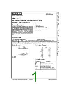
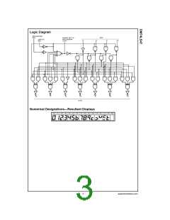
Functional Description
The DM74LS47 decodes the input data in the pattern indi-
cated in the Truth Table and the segment identification
illustration. If the input data is decimal zero, a LOW signal
applied to the RBI blanks the display and causes a multi-
digit display. For example, by grounding the RBI of the
highest order decoder and connecting its BI/RBO to RBI of
the next lowest order decoder, etc., leading zeros will be
suppressed. Similarly, by grounding RBI of the lowest order
decoder and connecting its BI/RBO to RBI of the next high-
est order decoder, etc., trailing zeros will be suppressed.
Leading and trailing zeros can be suppressed simulta-
neously by using external gates, i.e.: by driving RBI of a
intermediate decoder from an OR gate whose inputs are
BI/RBO of the next highest and lowest order decoders. BI/
RBO also serves as an unconditional blanking input. The
internal NAND gate that generates the RBO signal has a
resistive pull-up, as opposed to a totem pole, and thus BI/
RBO can be forced LOW by external means, using wired-
collector logic. A LOW signal thus applied to BI/RBO turns
off all segment outputs. This blanking feature can be used
to control display intensity by varying the duty cycle of the
blanking signal. A LOW signal applied to LT turns on all
segment outputs, provided that BI/RBO is not forced LOW.
www.fairchildsemi.com
2

 FAIRCHILD [ FAIRCHILD SEMICONDUCTOR ]