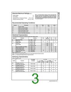
Absolute Maximum Ratings(Note 1)
Note 1: The “Absolute Maximum Ratings” are those values beyond which
the safety of the device cannot be guaranteed. The device should not be
operated at these limits. The parametric values defined in the Electrical
Characteristics tables are not guaranteed at the absolute maximum ratings.
The “Recommended Operating Conditions” table will define the conditions
for actual device operation.
Supply Voltage
Input Voltage
7V
7V
Operating Free Air Temperature Range
Storage Temperature Range
0°C to +70°C
−65°C to +150°C
Recommended Operating Conditions
Symbol
Parameter
Min
4.75
2
Nom
Max
Units
V
VCC
VIH
VIL
IOH
IOL
TA
Supply Voltage
5
5.25
HIGH Level Input Voltage
LOW Level Input Voltage
HIGH Level Output Current
LOW Level Output Current
Free Air Operating Temperature
V
0.8
−0.4
8
V
mA
mA
°C
0
70
Electrical Characteristics
over recommended operating free air temperature range (unless otherwise noted)
Symbol Parameter Conditions
Input Clamp Voltage = Min, I = −18 mA
Typ
Min
Max
Units
(Note 2)
V
V
V
V
V
V
V
−1.5
V
V
I
CC
CC
I
HIGH Level
= Min, I = Max
OH
OH
2.7
3.4
Output Voltage
LOW Level
= Max, V = Min
IH
IL
V
= Min, I = Max
0.25
0.35
0.25
0.4
0.5
OL
CC
OL
Output Voltage
= Max, V = Min
V
IL
IH
I
= 4 mA, V = Min
0.4
OL
CC
I
I
I
I
I
Input Current @ Max Input Voltage
HIGH Level Input Current
LOW Level Input Current
Short Circuit Output Current
Supply Current
V
V
V
V
V
= Max, V = 7V
0.1
mA
µA
I
CC
CC
CC
CC
CC
I
= Max, V = 2.7V
20
IH
I
= Max, V = 0.4V
−0.4
−100
14
mA
mA
mA
IL
I
= Max (Note 3)
= Max (Note 4)
−20
OS
CC
9
Note 2: All typicals are at V = 5V, T = 25°C.
CC
A
Note 3: Not more than one output should be shorted at a time, and the duration should not exceed one second.
Note 4: I is measured with all outputs OPEN and all inputs GROUNDED.
CC
Switching Characteristics
at VCC = 5V and T = 25°C
A
R
= 2 kΩ
From (Input)
L
C
= 15 pF
C = 50 pF
L
Symbol
Parameter
To (Output)
Units
L
Min
Max
Min
Max
t
t
t
t
Propagation Delay Time
LOW-to-HIGH Level Output
Propagation Delay Time
HIGH-to-LOW Level Output
Propagation Delay Time
LOW-to-HIGH Level Output
Propagation Delay Time
HIGH-to-LOW Level Output
PLH
Data to Output
Data to Output
Strobe to Output
Strobe to Output
30
30
20
25
35
ns
ns
ns
ns
PHL
PLH
PHL
35
25
35
3
www.fairchildsemi.com

 FAIRCHILD [ FAIRCHILD SEMICONDUCTOR ]