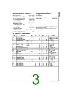
Absolute Maximum Ratings(Note 1)
Recommended Operating
Conditions
Storage Temperature
−65°C to +150°C
Ambient Temperature under Bias
Junction Temperature under Bias
VCC Pin Potential to Ground Pin
Input Voltage (Note 2)
−55°C to +125°C
−55°C to +150°C
−0.5V to +7.0V
Free Air Ambient Temperature
Supply Voltage
0°C to +70°C
+4.5V to +5.5V
−0.5V to +7.0V
Input Current (Note 2)
−30 mA to +5.0 mA
Voltage Applied to Output
in HIGH State (with VCC = 0V)
Standard Output
−0.5V to VCC
Note 1: Absolute maximum ratings are values beyond which the device
may be damaged or have its useful life impaired. Functional operation
under these conditions is not implied.
3-STATE Output
−0.5V to +5.5V
Current Applied to Output
in LOW State (Max)
Note 2: Either voltage limit or current limit is sufficient to protect inputs.
twice the rated IOL (mA)
4000V
ESD Last Passing Voltage (Min)
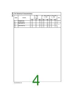
DC Electrical Characteristics
V
Symbol
Parameter
Input HIGH Voltage
Min
Typ
Max
Units
Conditions
CC
V
V
V
V
2.0
V
V
V
V
Recognized as a HIGH Signal
Recognized as a LOW Signal
IH
Input LOW Voltage
0.8
IL
Input Clamp Diode Voltage
Output HIGH Voltage
−1.2
Min
Min
I
I
I
I
I
I
= −18 mA
CD
OH
IN
10% V
10% V
2.4
2.0
2.7
= −3 mA (A )
n
CC
OH
OH
OH
OL
OL
= −15 mA (B )
CC
n
5% V
= −3 mA (A )
n
CC
V
Output LOW Voltage
Input HIGH Current
10% V
10% V
0.5
0.55
5.0
V
Min
= 24 mA (A )
n
OL
CC
CC
= 64 mA (B )
n
I
I
I
I
µA
µA
mA
µA
V
Max
Max
Max
Max
0.0
V
= 2.7V
IH
IN
Input HIGH Current Breakdown Test
7.0
V
V
V
= 7.0V (OE, T/R)
BVI
IN
Input HIGH Current Breakdown (I/O)
Output HIGH Leakage Current
Input Leakage
0.5
50
= 5.5 V (A , B )
n n
BVIT
CEX
IN
= V (A , B )
OUT
CC
n
n
V
4.75
I
= 1.9 µA
ID
ID
OD
IL
Test
All Other Pins Grounded
V = 150 mV
IOD
I
Output Leakage
3.75
µA
0.0
Circuit Current
All Other Pins Grounded
I
Input LOW Current
−1.2
mA
Max
V
V
V
V
V
V
V
V
V
= 0.5V (T/R, OE)
IN
I
I
I
+ I
Output Leakage Current
Output Leakage Current
Output Short-Circuit Current
70
−650
−150
−225
500
90
µA
µA
Max
Max
Max
= 2.7V (A , B )
n n
IH
IL
OZH
OUT
OUT
OUT
OUT
OUT
+ I
= 0.5V (A , B )
n n
OZL
−60
mA
= 0V (A )
n
OS
−100
= 0V (B )
n
I
I
I
I
Bus Drainage Test
µA
mA
mA
mA
0.0V
Max
Max
Max
= 5.25V(A , B )
n n
ZZ
Power Supply Current
Power Supply Current
Power Supply Current
70
95
85
= HIGH
CCH
CCL
CCZ
O
O
O
120
110
= LOW
= HIGH Z
3
www.fairchildsemi.com

 FAIRCHILD [ FAIRCHILD SEMICONDUCTOR ]