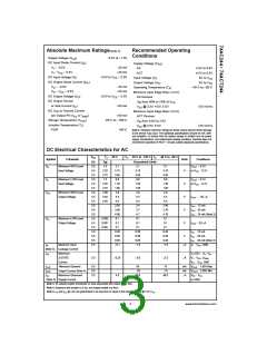
Absolute Maximum Ratings(Note 2)
Recommended Operating
Conditions
Supply Voltage (VCC
DC Input Diode Current (IIK
VI 0.5V
)
0.5V to 7.0V
)
Supply Voltage (VCC
)
20 mA
20 mA
AC
2.0V to 6.0V
4.5V to 5.5V
0V to VCC
VI VCC 0.5V
ACT
DC Input Voltage (VI)
0.5V to VCC 0.5V
Input Voltage (VI)
Output Voltage (VO)
DC Output Diode Current (IOK
VO 0.5V
)
0V to VCC
20 mA
20 mA
Operating Temperature (TA)
Minimum Input Edge Rate ( V/ t)
AC Devices
40 C to 85 C
VO VCC 0.5V
DC Output Voltage (VO)
DC Output Source
0.5V to VCC 0.5V
V
IN from 30% to 70% of VCC
or Sink Current (IO)
50 mA
VCC @ 3.3V, 4.5V, 5.5V
Minimum Input Edge Rate ( V/ t)
ACT Devices
125 mV/ns
125 mV/ns
DC VCC or Ground Current
per Output Pin (ICC or IGND
)
50 mA
Storage Temperature (TSTG
Junction Temperature (TJ)
PDIP
)
65 C to 150 C
VIN from 0.8V to 2.0V
VCC @ 4.5V, 5.5V
140 C
Note 2: Absolute maximum ratings are those values beyond which damage
to the device may occur. The databook specifications should be met, with-
out exception, to ensure that the system design is reliable over its power
supply, temperature, and output/input loading variables. Fairchild does not
recommend operation of FACT circuits outside databook specifications.
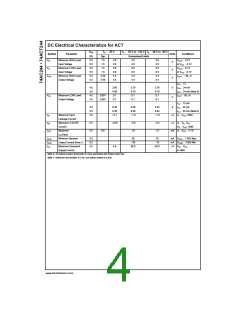
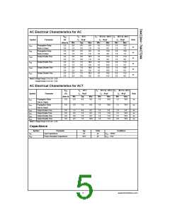
DC Electrical Characteristics for AC
V
T
25 C
T
55 C to 125 C
T
A
40 C to 85 C
CC
A
A
Symbol
Parameter
Units
Conditions
(V)
3.0
4.5
5.5
3.0
4.5
5.5
3.0
4.5
5.5
3.0
4.5
5.5
3.0
4.5
5.5
3.0
4.5
5.5
5.5
Typ
1.5
Guaranteed Limits
V
Minimum HIGH Level
Input Voltage
2.1
2.1
3.15
3.85
0.9
2.1
3.15
3.85
0.9
V
0.1V
0.1V
IH
OUT
2.25
2.75
1.5
3.15
3.85
0.9
V
or V
CC
V
Maximum LOW Level
Input Voltage
V
0.1V
0.1V
IL
OUT
2.25
2.75
2.99
4.49
5.49
1.35
1.65
2.9
1.35
1.65
2.9
1.35
1.65
2.9
V
V
V
V
or V
CC
V
Minimum HIGH Level
Output Voltage
OH
4.4
4.4
4.4
I
50 A
OUT
5.4
5.4
5.4
2.56
3.86
4.86
0.1
2.4
2.46
3.76
4.76
0.1
I
I
I
12 mA
24 mA
OH
OH
OH
3.7
4.7
24 mA (Note 3)
V
Maximum LOW Level
Output Voltage
0.002
0.001
0.001
0.1
OL
0.1
0.1
0.1
I
50 A
OUT
0.1
0.1
0.1
0.36
0.36
0.36
0.1
0.50
0.50
0.50
1.0
0.44
0.44
0.44
1.0
I
I
I
12 mA
OL
OL
OL
V
A
24 mA
24 mA (Note 3)
I
Maximum Input
V
V
, GND
IN
I
CC
(Note 5) Leakage Current
I
Maximum
V (OE)
V
, V
OZ
I
IL IH
3-STATE
5.5
0.25
5.0
2.5
A
V
V
V
V
V
V
, V
GND
I
CC
Current
V
, GND
O
CC
I
Minimum Dynamic
Output Current (Note 4)
Maximum Quiescent
5.5
5.5
5.5
50
50
75
75
mA
mA
A
1.65V Max
3.85V Min
OLD
OLD
I
OHD
OHD
IN
I
4.0
80.0
40.0
V
CC
CC
(Note 5) Supply Current
or GND
Note 3: All outputs loaded; thresholds on input associated with output under test.
Note 4: Maximum test duration 2.0 ms, one output loaded at a time.
Note 5: I and I @ 3.0V are guaranteed to be less than or equal to the respective limit @ 5.5V V .
CC
IN
CC
3
www.fairchildsemi.com

 FAIRCHILD [ FAIRCHILD SEMICONDUCTOR ]