Document No.: FT_000288
FT232H SINGLE CHANNEL HI-SPEED USB TO MULTIPURPOSE UART/FIFO IC
Datasheet Version 1.8
Clearance No.: FTDI #199
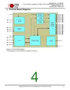
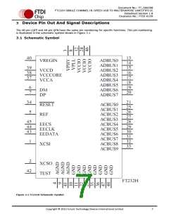
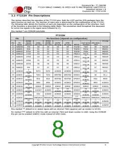
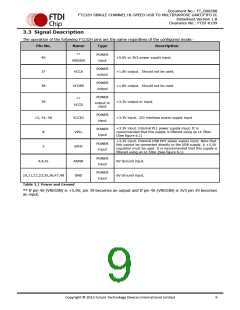
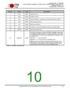
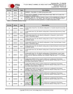
3.2 FT232H Pin Descriptions
This section describes the operation of the FT232H pins. Both the LQFP and the QFN packages have the
same function on each pin. The function of many pins is determined by the configuration of the FT232H.
The following table details the function of each pin dependent on the configuration of the interface. Each
of the functions is described in the following table (Note: The convention used throughout this document
for active low signals is the signal name followed by #).
Pins marked * are EEPROM selectable
FT232H
Pin
Pin functions (depends on configuration)
ASYNC
Serial
(RS232)
STYLE
ASYNC
245 FIFO
FT1248
Pin
#
Pin
Name
SYNC
245 FIFO
ASYNC
Bit-bang
SYNC
Bit-bang
Fast Serial CPU Style
MPSSE
interface
FIFO
13 ADBUS0
14 ADBUS1
15 ADBUS2
16 ADBUS3
TXD
RXD
D0
D1
D2
D3
D0
D1
D2
D3
D0
D1
D2
D3
D0
D1
D2
D3
TCK/SK
FSDI
D0
MIOSI0
MIOSI1
MIOSI2
MIOSI3
TDI/DO
TDO/DI
TMS/CS
FSCLK
FSDO
D1
D2
D3
RTS#
CTS#
FSCTS
**
TriSt-UP
**
17 ADBUS4
18 ADBUS5
19 ADBUS6
20 ADBUS7
21 ACBUS0
25 ACBUS1
26 ACBUS2
DTR#
DSR#
DCD#
RI#
D4
D5
D4
D5
D4
D5
D4
D5
GPIOL0
GPIOL1
GPIOL2
GPIOL3
GPIOH0
GPIOH1
GPIOH2
D4
D5
MIOSI4
MIOSI5
MIOSI6
MIOSI7
SCLK
TriSt-UP
**
TriSt-UP
**
D6
D6
D6
D6
D6
D7
D7
D7
D7
D7
TriSt-UP
*
**
ACBUS0
**
ACBUS1
**
ACBUS2
**
ACBUS3
RXF#
TXE#
RD#
RXF#
TXE#
RD#
ACBUS0
WRSTB#
RDSTB#
ACBUS0
WRSTB#
RDSTB#
CS#
A0
TXDEN
**
SS_n
ACBUS1
**
ACBUS2
*
RXLED#
*
TXLED#
**
RD#
MISO
27 ACBUS3
28 ACBUS4
29 ACBUS5
30 ACBUS6
31 ACBUS7
32 ACBUS8
33 ACBUS9
WR#
SIWU#
CLKOUT
OE#
WR#
ACBUS3
SIWU#
ACBUS3
SIWU#
GPIOH3
GPIOH4
GPIOH5
GPIOH6
WR#
ACBUS3
ACBUS4
ACBUS5
ACBUS6
SIWU#
ACBUS5
ACBUS6
SIWU#
SIWU#
**
ACBUS5
**
ACBUS5
**
**
ACBUS5
**
ACBUS6
ACBUS5
**
ACBUS5
**
ACBUS6
ACBUS6
ACBUS6
ACBUS6
***
GPIOH7
PWRSAV# PWRSAV# PWRSAV# PWRSAV#
PWRSAV# PWRSAV# PWRSAV#
PWRSAV#
**
ACBUS8
**
ACBUS9
**
**
**
**
**
**
**
ACBUS8
ACBUS9
ACBUS8
**
ACBUS8
**
ACBUS8
**
ACBUS8
**
ACBUS8
**
ACBUS8
**
ACBUS8
**
ACBUS9
ACBUS9
ACBUS9
ACBUS9
ACBUS9
ACBUS9
ACBUS9
Pins marked ** default to tri-stated inputs with an internal 75KΩ (approx) pull up resistor to VCCIO.
Pin marked *** default to GPIO line with an internal 75KΩ pull down resistor to GND. Using the EEPROM
this pin can be enabled USBVCC mode instead of GPIO mode.
Copyright © 2012 Future Technology Devices International Limited
8

 ETC [ ETC ]