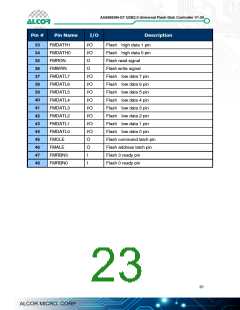
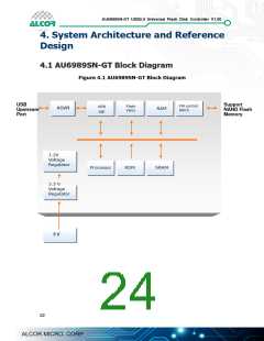
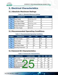
AU6989SN-GT USB2.0 Universal Flash Disk Controller V1.00
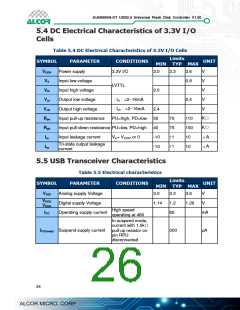
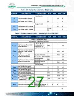
Table 5.6 Static characteristic:Digital pin
SYMBOL
PARAMETER
CONDITIONS
MIN TYP MAX UNIT
Input levels
VIL
VIH
Low-level input voltage
High-level input voltage
0.8
V
V
2.0
Output levels
VOL
VOH
Low-level output voltage
High-level output voltage
0.2
V
V
VDDH-
0.2
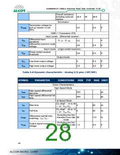
Table 5.7 Static characteristic:Analog I/O pins(DP/DM)
SYMBOL
PARAMETER
CONDITIONS
MIN TYP MAX UNIT
USB2.0 Transceiver (HS)
Input Levels (differential receiver)
VI -VI
DP
DM
High speed differential
input sensitivity
measured at the
connection as
application circuit
VHSDIFF
300
mV
mV
High speed data signaling
VHSCM common mode voltage
range
-50
500
100
Squelch detected
mV
mV
High speed squelch
VHSSQ
detection threshold
No squelch detected 150
Disconnection
625
mV
mV
High speed disconnection detected
detection threshold
VHSDSC
Disconnection not
detected
525
Output Levels
High speed idle level
output voltage(differential)
High speed low level
output voltage(differential)
High speed high level
output voltage(differential)
Chirp-J output voltage
differential
VHSOI
VHSOL
-10
10
mV
mV
mV
-10
10
VHSOH
VCHIRPJ
VCHIRPK
360
700
440
1100 mV
Chirp-K output voltage
differential
-900
-500
mV
Resistance
Equivalent
resistance used as 3
internal chip only
RDRV
Driver output impedance
6
9
25

 ETC [ ETC ]